2 layers
 lzptr/solar-controller
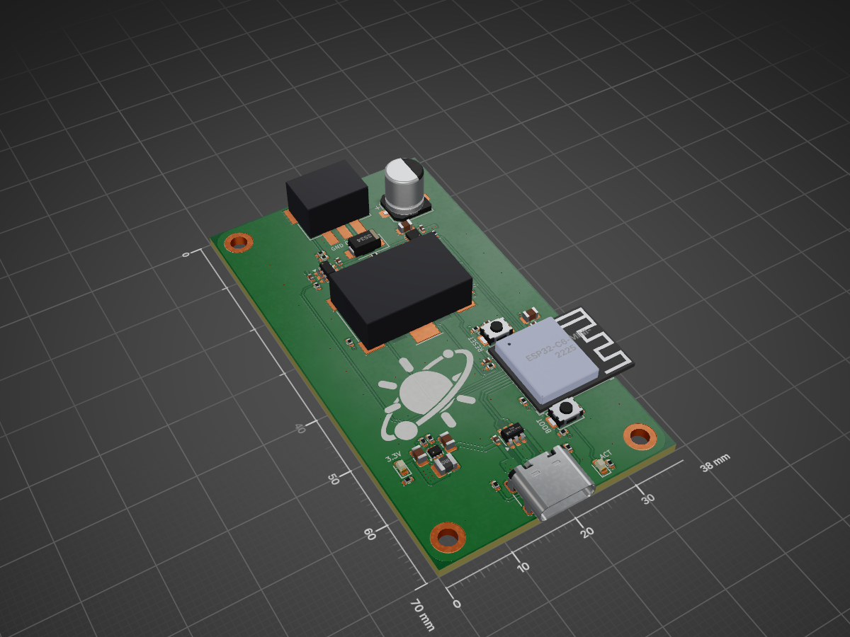
ESP32 Based PCB for Controlling a Solar System Light Chain
Solar controller is an open-source printed circuit board by lzptr, from the lzptr/solar-controller repository on GitHub. It is a 4-layer board of 38 × 70 mm with 53 parts on 53 nets, routed with 204 tracks and 100 vias.
It is built around the ESP32-C6-MINI-1U-H4, TPS62A01ADRL and SN74LVC1T45DBVRE4, with the USBLC6-2SC6, MA10V470M6X8 and EC11J1525402 among its other parts. Its parts include 21 resistors, 13 capacitors, 5 ICs, 3 diodes and 3 switches. It belongs with the power boards and the ESP32 and RISC-V boards of this library.


Small adapter PCB that sits back-to-back on the off-the-shelf 23 mm ring with seven SK6812 RGBW LEDs used in each planet globe. It gives the ring a keyed, pluggable connector so the cables between the globes can be made and changed later instead of being soldered to the ring at the final length.
globe interior
  ┆  LEDs face the globe
  ├─ LED ring (D23, 1.6 mm, LEDs 1.6 mm tall)
  ├─ adapter (this board, 1.6 mm)   back-to-back with the ring, pads aligned
  └─ J1  PHD 2.0 mm 2x3 wafer      points away from the globe, into the socket
         cable from the previous globe (odd pins) / cable to the next globe (even pins)
Five standard header pins (0.64 mm square, pulled out of a pin header strip) go through both boards and carry IN, 5V, GND, GND and OUT; 5V and GND are bussed straight through the adapter, data enters the ring at IN and leaves it at OUT. Two M2.5 screws through the shared 2.9 mm holes clamp the stack into the printed socket.
| File | Content |
|---|---|
led_adapter.kicad_pro/_sch/_pcb | KiCad 10 project, created from the JLCPCB 1-2 layer template |
LedAdapter.kicad_sym | symbol LED_Ring_SK6812_7 (the ring as a 5-pin module) |
LedAdapter.pretty/Hanxia_HX-PHD2.0-2x3ALT.kicad_mod | connector footprint from the manufacturer land pattern |
LedAdapter.pretty/LED_Ring_SK6812_7_D23_Pins.kicad_mod | the ring's pad pattern (pins) and mounting holes |
datasheets/ | connector drawing |
Ring: 23.0 mm diameter, 1.6 mm thick, 3.2 mm with LEDs. Mounting holes 2.9 mm, 19.2 mm apart, on the x axis. Pad positions, seen from the LED side with the holes left/right (origin = ring centre, y up):
| Pad | x | y |
|---|---|---|
| IN | +2.54 | +4.57 |
| 5V (PWR) | -2.54 | +4.57 |
| GND | -5.33 | 0.00 |
| GND | -2.54 | -4.57 |
| OUT | +2.54 | -4.57 |
The adapter is viewed from the connector side, i.e. the ring is seen from its back, so on the adapter the pattern is mirrored: IN top-left, 5V top-right, GND right, GND bottom-right, OUT bottom-left (as labelled on the silkscreen).
Positions were measured from the seller's front and back product photos scaled to the 19.2 mm hole pitch and confirmed with calipers on the real ring: IN to OUT 9.1 mm, IN to PWR 5.1 mm (model: 9.14 / 5.08). The pattern's position relative to the mounting holes comes from the photos (about 0.2 mm uncertainty), which the 0.4 mm clearance of M2.5 screws in the 2.9 mm holes covers. The ring's pads are 1.6 mm with a hole that takes a standard 0.64 mm square header pin; the adapter's pin holes are 1.2 mm (2.0 mm pad) so the pins pass both boards with some slack.
hanxia HX-PHD2.0-2x3ALT, LCSC C53055815, JLCPCB extended part (435 in stock on 2026-10-20). 2x3 top-entry SMD wafer, 2.0 mm pitch, JST PHD compatible, keyed, 3 A per contact, housing 8.0 x 5.55 mm, 8.1 mm tall.
Mating side: JST PHDR-06VS housing with SPHD-001T-P0.5 contacts (AWG 22 to 28) or the equivalent "PHD2.0 2x3" clone housings and crimp terminals.
Same land pattern, usable as drop-in alternatives if the stock runs out: SHOU HAN PHD2.0-2x3PLT (C48783195), XUNPU WAFER-PHD2.0-6PLB (C55130937). A 2.54 mm 2x3 SMD pin header (hanxia HX PZ2.54-2x3P TP, C32713283, 44k in stock) would also fit the board with a new footprint, but it is not keyed.
Pinout (odd row = cable from the previous globe or the controller, even row = cable to the next globe; the pin-1 mark is next to the odd data pin):
| Pin | Row | Signal |
|---|---|---|
| 1 | odd | DIN (to the ring's IN) |
| 2 | even | DOUT (from the ring's OUT) |
| 3 | odd | GND |
| 4 | even | GND |
| 5 | odd | +5V |
| 6 | even | +5V |
The connector is shifted 0.8 mm towards the DIN/DOUT side so its solder tails clear the right-hand GND pin pad. Its housing ends cover the inner 0.4 mm of the four outer pin pads; the holes themselves and the outer half of each pad stay free, which is enough to solder the pins from the outside.
Board: 23 mm round, 2 layers, 1.6 mm, JLCPCB rules from the template. For the
JLCPCB BOM/CPL use the Fabrication Toolkit plugin as for the controller board;
J1 carries the LCSC Part # field, J2 (the ring interface) is excluded from
BOM and position files.
| Qty | Value | Footprint | References |
|---|---|---|---|
| 7 | 100n | Capacitor_SMD:C_0402_1005Metric | C302, C304, C401, C402, C403, C407, C408 |
| 6 | 10k | Resistor_SMD:R_0402_1005Metric | R301, R302, R303, R404, R408, R413 |
| 6 | 2k2 | Resistor_SMD:R_0402_1005Metric | R211, R306, R405, R406, R411, R412 |
| 4 | 100k | Resistor_SMD:R_0402_1005Metric | R208, R407, R410, R414 |
| 4 | GND | MountingHole:MountingHole_2.7mm_M2.5_ISO14580_Pad | H101, H102, H103, H104 |
| 3 | 22u | Capacitor_SMD:C_0805_2012Metric | C206, C303, C405 |
| 2 | 5k1 | Resistor_SMD:R_0402_1005Metric | R307, R308 |
| 1 | 1k | Resistor_SMD:R_0402_1005Metric | R403 |
| 1 | 1u | Capacitor_SMD:C_0402_1005Metric | C301 |
| 1 | 1u | Inductor_SMD:L_1008_2520Metric | L201 |
| 1 | 22k | Resistor_SMD:R_0402_1005Metric | R209 |
| 1 | 330 | Resistor_SMD:R_0402_1005Metric | R409 |
| 1 | 470u | Capacitor_SMD:CP_Elec_6.3x7.7 | C404 |
| 1 | 4u7 | Capacitor_SMD:C_0805_2012Metric | C205 |
| 1 | BOOT | Button_Switch_SMD:SW_SPST_TS-1088-xR020 | SW302 |
| 1 | EC11J1525402 | SolarController:ALPS_EC11J1525402 | SW402 |
| 1 | ESP32-C6-MINI-1U-H4 | PCM_Espressif:ESP32-C6-MINI-1U | U301 |
| 1 | LED_ACT | LED_SMD:LED_0603_1608Metric | D301 |
| 1 | LED_GREEN | LED_SMD:LED_0603_1608Metric | D201 |
| 1 | LOGO | LOGO | G*** |
| 1 | RESET | Button_Switch_SMD:SW_SPST_TS-1088-xR020 | SW301 |
| 1 | SN74LVC1T45DBVR | Package_TO_SOT_SMD:SOT-23-6 | U403 |
| 1 | SS34 | Diode_SMD:D_SMA | D401 |
| 1 | TPS259531DSGR | Package_SON:Texas_DSG0008A_WSON-8-1EP_2x2mm_P0.5mm_EP0.9x1.6mm | U402 |
| 1 | TPS62A01ADRL | Package_TO_SOT_SMD:SOT-563 | U203 |
| 1 | USBLC6-2SC6 | Package_TO_SOT_SMD:SOT-23-6 | U302 |
| 1 | USB_C_Receptacle_USB2.0 | Connector_USB:USB_C_Receptacle_HRO_TYPE-C-31-M-12 | J301 |
| 1 | ZX-XH2.54-3PWT | SolarController:Megastar_ZX-XH2.54-3PWT | J401 |
It measures 38 × 70 mm and has 4 copper layers, 1.65 mm thick.
53 parts, built around the ESP32-C6-MINI-1U-H4, TPS62A01ADRL, SN74LVC1T45DBVRE4 and USBLC6-2SC6. The full list of its parts is on this page, with links to each part's symbol and footprint where PCBKit's library has them.
From the lzptr/solar-controller repository on GitHub, at the commit this page was made from: the board is hardware/solar_controller/solar-controller.kicad_pcb and its schematic hardware/led_adapter/led_adapter.kicad_sch. PCBKit opens the board in the browser, with nothing to install.
Its repository states no licence, so its author keeps all rights: ask lzptr before reusing the design.


steven-na/saria
An rp2040 based, wired, split-ergo, mechanical keyboard. Running on QMK firmware

Janky-Jingle-Crew/SouthPoleLevitator
2025 Christmas card "South Pole Levitator"


