2 layers144.9 × 59.8 mm
Monkeys
PacketChat/MonkeyBadge
This repository contains the hardware design files, badge code, and backend infrastructure code for the HushCon Winter 2023 badge.
153 parts21

 luthfai/meshthingy
KiCad 10 · 2-layer · 71 × 46 mm · ESP32-S3 + SX1262 LoRa · USB-C · Li-Ion · hardware rev R1
Meshthingy is an open-source printed circuit board by luthfai, from the luthfai/meshthingy repository on GitHub. It is a 2-layer board of 71 × 46 mm with 96 parts on 84 nets, routed with 808 tracks and 378 vias.
It is built around the ESP32-S3-WROOM-1-N8, BME280 and TPS62046DGQR, with the AT24C32AN/HG, BQ24072RGTR and 1N4148WS among its other parts. Its parts include 24 resistors, 23 capacitors, 10 ICs, 8 diodes and 4 transistors. It belongs with the ESP32 boards of this library.


An off-grid LoRa mesh communicator — a pocket-sized ESP32-S3 node that sends text and GPS position over kilometres of open ground, with no cell tower, no SIM, no subscription, and no internet.
KiCad 10 · 2-layer · 71 × 46 mm · ESP32-S3 + SX1262 LoRa · USB-C · Li-Ion · hardware rev R1
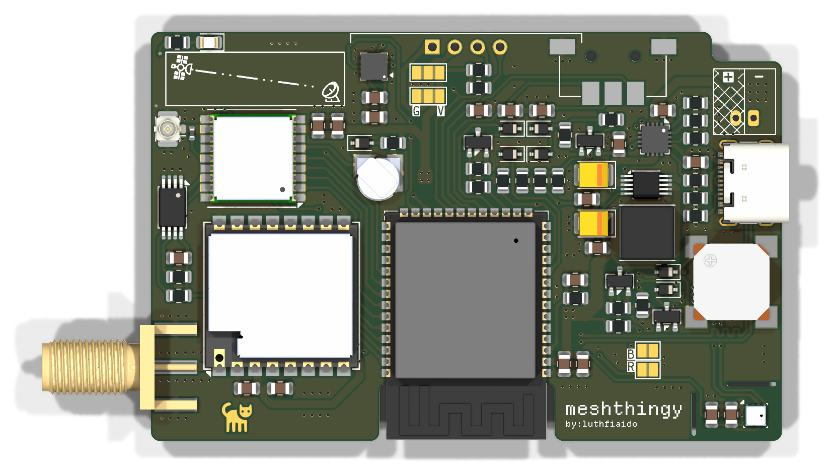
[!WARNING] Rev R1 is currently in fabrication — nothing here has been tested yet. The schematic and layout are finished and pass DRC, but no board has been assembled or powered up. Everything in this README (pin map, charger settings, power latch behaviour, assembly notes) describes the design as intended and may change after bring-up. Build one at your own risk.
| Stage | Status |
|---|---|
| Schematic | ✅ Done |
| PCB layout | ✅ Done — 0 DRC violations, 0 unconnected items |
| BOM | ✅ Done — a few part variants still to pick (see Bill of materials) |
| PCB fabrication | ⏳ In progress |
| Assembly | ⬜ Not started |
| Bring-up and testing | ⬜ Not started |
| Firmware | 🚧 Work in progress |
Phones stop working the moment you leave coverage. meshthingy doesn't need coverage — it is the network.
Each board is one node in a self-healing Meshtastic mesh. Nodes talk directly to each other over licence-free LoRa radio, and every node automatically relays traffic for its neighbours. Two units give you a private long-range walkie-talkie for text; a handful scattered across a valley, a campsite, a ridgeline, or a city block give everyone in that area a shared messaging network that keeps working when nothing else does.
Because LoRa trades bandwidth for range and power, a node runs for days on a small Li-Ion cell and reaches several kilometres line-of-sight — far past Wi-Fi or Bluetooth, and without the power budget a cellular radio demands.
Typical uses: hiking and backcountry trips, sailing, off-road convoys, festival and event crews, neighbourhood emergency preparedness, and as a low-cost long-range telemetry link for remote sensors.
The onboard GPS, environmental and motion sensors mean a node is useful even with nobody holding it — drop one on a hilltop as a solar-powered repeater and it becomes a weather station that also extends everyone's range.
flowchart TB
    subgraph RF["📡 Radio"]
        LORA["<b>U4 · HT-RA62</b><br/>SX1262 LoRa"]
        SMA["J4 · SMA<br/>edge mount"]
        LORA --- SMA
    end

    subgraph CORE["🧠 Core"]
        MCU["<b>U7 · ESP32-S3-WROOM-1</b><br/>Wi-Fi · BLE · dual core"]
    end

    subgraph NAV["🛰️ Navigation"]
        GPS["<b>U2 · ATGM336H</b><br/>GNSS receiver"]
        UFL["J3 · U.FL<br/>active antenna"]
        EEP["U8 · AT24CS32<br/>EEPROM"]
        BAT2["C13 · XH414H<br/>backup cell"]
        UFL --- GPS
        GPS -->|"private I²C"| EEP
        BAT2 -.->|"keeps time"| GPS
    end

    subgraph IO["🔌 I²C peripherals"]
        OLED["U1 · 0.96in OLED"]
BME["U9 · BME280<br/>temp · humidity · pressure"]USB-C and the battery both feed a power-path charger, so the node keeps running while it charges and switches over seamlessly when USB is unplugged. The 3.3 V buck converter is only enabled while something holds the power latch on.
flowchart LR
    USB["<b>J1</b><br/>USB-C<br/>5 V in"] -->|VBUS| CHG
    BATT["<b>J2</b><br/>Li-Ion cell<br/>JST-PH"] <-->|charge / discharge| CHG
    CHG["<b>U6 · BQ24072</b><br/>Li-Ion charger<br/>+ power path"] -->|VSYS| BUCK
    LATCH["<b>Power latch</b><br/>Q2 · Q3"] -->|BUCK_EN| BUCK
    BUCK["<b>U3 · TPS62046</b><br/>3.3 V step-down<br/>via L2"] -->|"+3V3"| RAIL

    BTN["Lever push"] -.-> LATCH
    PG["USB present<br/>(PGOOD)"] -.-> LATCH
    HOLD["IO9 · SYS_EN<br/>(firmware hold)"] -.-> LATCH

    RAIL["<b>+3V3 rail</b>"] --> M1["ESP32-S3"]
    RAIL --> M2["LoRa"]
    RAIL --> M3["GNSS"]
    RAIL --> M4["Sensors + OLED"]
    RAIL --> M5["Buzzer + vib motor"]

    classDef src fill:#dc2626,stroke:#991b1b,color:#fff,stroke-width:2px
    classDef conv fill:#ea580c,stroke:#c2410c,color:#fff,stroke-width:2px
    classDef rail fill:#16a34a,stroke:#15803d,color:#fff,stroke-width:2px
    classDef load fill:#475569,stroke:#334155,color:#fff
    classDef ctl fill:#64748b,stroke:#475569,color:#fff
    class USB,BATT src
class CHG,BUCK convThe buck converter's enable is driven by a PNP switch (Q2) from a latch node
that is pulled low by any one of three sources, each isolated by a 1N4148WS:
U5, D7) — pressing it powers the board up.PGOOD from U6, D4) — the node is always on while plugged in.IO9 / SYS_EN through Q3) — firmware must drive IO9 high
early in boot, or the board switches off again when the lever is released.
Driving IO9 low (with USB unplugged) powers the node down.The MCU can read the lever push on IO10 and USB presence on IO17 (both through
diodes, active low, use internal pull-ups). The latch diodes must stay
low-leakage silicon parts — Schottkys leak enough to half-enable the buck when off.
| Setting | Part | Value |
|---|---|---|
| Fast-charge current | R4 = 1k (1%) | ≈ 890 mA |
| USB input current limit | R5 = 1k2, EN2 = 1 / EN1 = 0 | ≈ 1.34 A |
| Safety timers | R6 = 47k | pre-charge ≈ 38 min, fast charge ≈ 6.3 h |
| Termination | TD tied low | enabled |
| Battery temperature | R3 = 10k fixed on TS | no thermistor, sensing disabled |
| Charge enable | IO18 (R7 pull-down) | low = charging allowed |
VSYS follows the battery (and tracks VBAT + 225 mV while charging). IO8 reads
VSYS / 2 through R16/R17 — that is the battery voltage when running on battery.
| Dimensions | 71.0 × 46.0 mm, cut-out under the ESP32 antenna, milled slots isolating the BME280 |
| Stackup | 2 layers (F.Cu / B.Cu), 1.6 mm |
| Components | 96 footprints, 353 pads (329 SMD, 22 through-hole, 2 NPTH), 378 vias |
| Density | 66% front, 9% back — almost everything lives on the front |
| Copper | GND pour on both layers, pour cut back under the RF connectors and antennas |
| Design rules | 0.175 mm clearance, 0.2 mm minimum track, 0.6 / 0.3 mm vias |
| Assembly | SMD on the front, 0805 passives; through-hole only for J2, the OLED header and the USB-C shell tabs |
Everything routes on two layers, which keeps this a cheap board to order from any prototype fab at standard tolerances.
|
Front — LoRa and GNSS modules, ESP32-S3, USB-C, buzzer, GPS backup cell, motor driver |
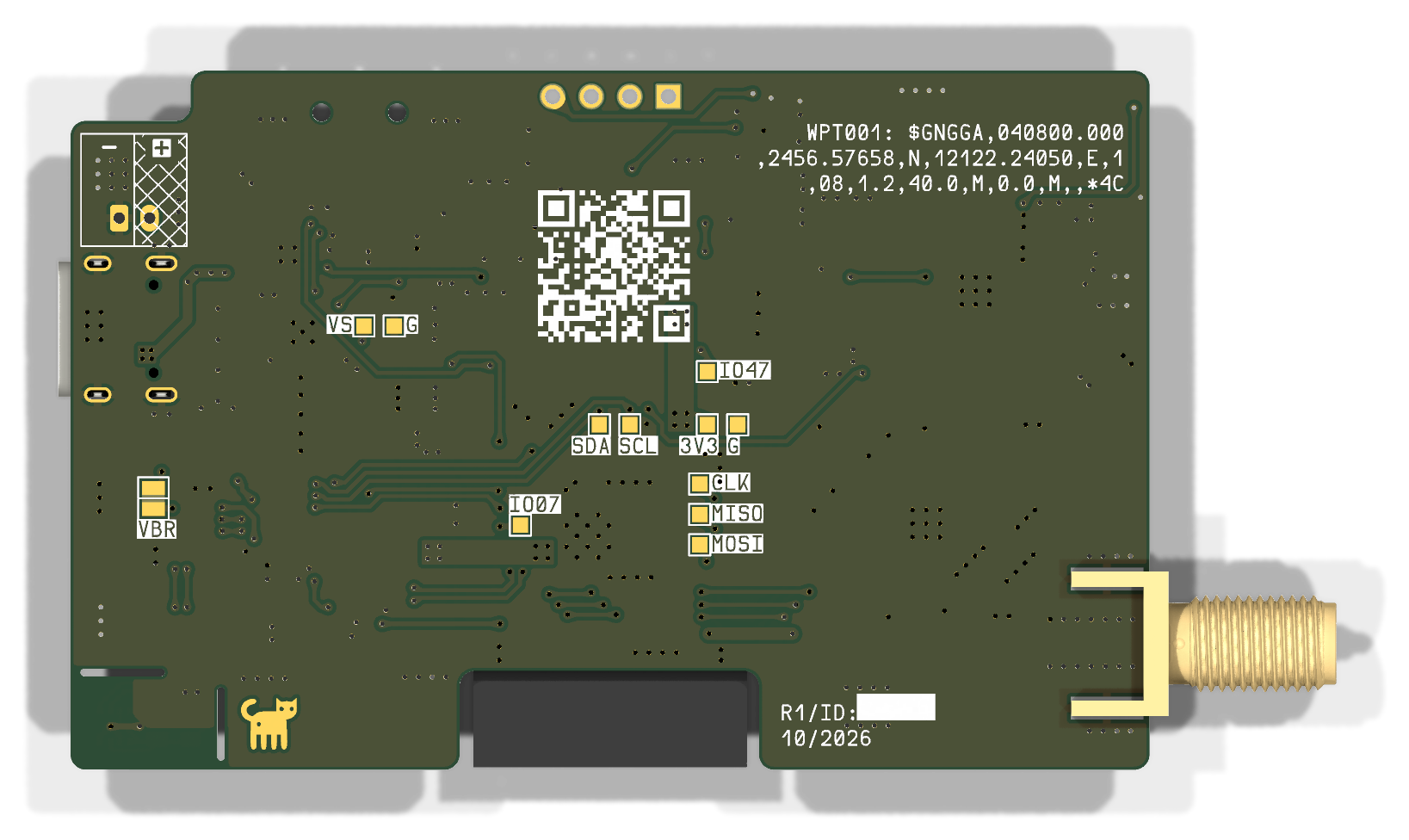 Back — labelled test points for every bus, vibration motor pads ( JP1, silkscreen VBR), repo QR code
|
Copper, silkscreen and board outline, plotted straight from the layout. The back view is mirrored so its silkscreen reads the right way round.
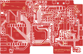 F.Cu + F.SilkS — signal routing over the front ground pour; B/R are the boot and reset pads
|
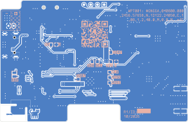 B.Cu + B.SilkS — mirrored; back pour with the test-point field and motor pads |
The RF section is deliberately sparse: the pours are cut back under the antenna connectors, the ESP32's PCB antenna hangs over a board cut-out, and the GPS keepout is marked on the silkscreen so nothing gets placed under it during assembly.
Regenerate the 3D renders and layer plots after any layout change (the renders are trimmed with ImageMagick):
kicad-cli pcb render --output /tmp/f.png --side top    --quality high --width 2000 --height 1300 meshthingy.kicad_pcb
kicad-cli pcb render --output /tmp/b.png --side bottom --quality high --width 2000 --height 1300 meshthingy.kicad_pcb
magick /tmp/f.png -trim +repage -bordercolor none -border 24 docs/meshthingy-f.png
magick /tmp/b.png -trim +repage -bordercolor none -border 24 docs/meshthingy-b.png

kicad-cli pcb export svg --output docs/layers-front.svg \
  --layers "F.Cu,F.SilkS,Edge.Cuts" \
  --page-size-mode 2 --exclude-drawing-sheet --check-zones --mode-single \
  meshthingy.kicad_pcb

kicad-cli pcb export svg --output docs/layers-back.svg \
  --layers "B.Cu,B.SilkS,Edge.Cuts" --mirror \
  --page-size-mode 2 --exclude-drawing-sheet --check-zones --mode-single \
meshthingy.kicad_pcb| Function | ESP32-S3 pin | Goes to |
|---|---|---|
| LoRa SCK | GPIO43 (TXD0) | U4 pin 12 SCK |
| LoRa MOSI | IO1 | U4 pin 14 MOSI |
| LoRa MISO | IO2 | U4 pin 13 MISO |
| LoRa CS | IO6 | U4 pin 15 NSS |
| LoRa DIO1 | IO4 | U4 pin 6 (IRQ) |
| LoRa RESET | IO5 | U4 pin 4 |
| LoRa BUSY | GPIO44 (RXD0) | U4 pin 10 |
| GPS TX → MCU RX | IO42 | U2 TXD |
| GPS RX ← MCU TX | IO41 | U2 RXD |
| GPS 1PPS | IO40 | U2 1PPS |
| GPS reset | IO38 | U2 nRESET |
| GPS on/off | IO39 | U2 ON/OFF |
| I²C SDA / SCL | IO13 / IO14 | OLED (0x3C), BME280 (0x76), LIS3DSH (0x1D) |
| Accelerometer INT | IO48 | U10 INT1 |
| Lever push | IO10 | U5 push, via D6 (active low) |
| Lever CCW / CW | IO11 / IO12 | U5 (active low, 100 nF debounce) |
| Power hold | IO9 | Q3 via R9 — drive high to stay on |
| USB present | IO17 | U6 PGOOD via D3 (active low) |
| Charge enable | IO18 | U6 CE (low = charge) |
| Battery sense | IO8 (ADC1_CH7) | VSYS / 2 |
| Vibration motor | IO15 | Q4 gate (10k pull-down R23) |
| Buzzer | IO16 | Q1 gate (10k pull-down R11) |
| Status LED | IO21 | D2 via R22 |
| USB D− / D+ | IO19 / IO20 | J1 (native USB) |
| Boot / reset | IO0 / EN | B / R pads |
| Spare / test | IO7, IO47 | back-side test points IO07, IO47 |
IO3, IO35–37, IO45 and IO46 are left unconnected (strapping pins and the octal-PSRAM pins on R8 module variants).
The design is hierarchical — root sheet meshthingy.kicad_sch:
| Sheet | Contents |
|---|---|
| Power Management | BQ24072 charger, TPS62046 buck, power latch, battery sense |
| Microcontroller | ESP32-S3-WROOM-1, boot and reset pads |
| LORA | HT-RA62 module and SMA antenna path |
| GPS | ATGM336H, U.FL antenna input, EEPROM, backup cell |
| Display | 0.96" OLED and its pinout-select jumpers |
| Air Sensors | BME280 |
| Accelerometer | LIS3DSH |
| Peripherals | Buzzer and vibration motor drivers, status LED, test points |
| Connectors | USB-C receptacle, JST-PH battery |
The curated BOM is bom/meshthingy-bom.csv: 36 board lines / 76 placed parts, plus the off-board items (battery, antennas, vibration motor). It adds manufacturer part numbers where the footprint fixes the part, and a notes column with ratings and the reason behind each value.
Still to pin down before ordering parts:
U7 — pick the module variant (e.g. -N8R2, -N16R8). Avoid the 1.8 V …V
variants: IO47 and IO48 are in use.C16, C25 — voltage rating (≥ 10 V low-ESR tantalum).U4 — HT-RA62-HF for 863–928 MHz, HT-RA62-LF for 433/470 MHz.Test points and solder jumpers are left out — they are PCB features, not parts.
A print-ready A4 copy with kitting checkboxes and the open items highlighted is
rendered from the CSV with python bom/render_bom_pdf.py (needs pip install weasyprint)
and written to bom/meshthingy-bom.pdf. For hand assembly, open
bom/ibom.html in a browser — an interactive BOM that highlights
each part's position on the board.
Open meshthingy.kicad_pro in KiCad 10 or newer.
All custom symbols and footprints live in libs/ and are referenced through
${KIPRJMOD}, so the project is self-contained — clone and open, nothing else to install.
Generate fabrication files from the command line:
# Gerbers + drill, ready to zip and upload to a fab
kicad-cli pcb export gerbers --output fab/ meshthingy.kicad_pcb
kicad-cli pcb export drill   --output fab/ meshthingy.kicad_pcb

# Raw schematic BOM and pick-and-place
kicad-cli sch export bom       --output fab/bom-raw.csv meshthingy.kicad_sch
kicad-cli pcb export pos       --output fab/pos.csv meshthingy.kicad_pcb

# Design rules check
kicad-cli pcb drc --output fab/drc.rpt meshthingy.kicad_pcb
Generated outputs are gitignored — regenerate them, or attach them to a release tag.
U3 (TPS62046) has a PowerPAD that must be soldered to the ground pad under it.
The pad is a copper shape on the board rather than part of the footprint, so it has
no paste aperture — tin it by hand, or add paste to the stencil, before reflowing U3.
JP3 and JP4 are three-way solder jumpers that select which OLED pin gets
+3V3 and which gets GND, so the footprint accepts display modules with either
pinout. They ship unbridged — bridge them to match the module you source
before expecting the display to light up. Never bridge all three pads of one jumper.
JP1 on the back (silkscreen VBR) is not a jumper. It's the pair of solder pads for the vibration
motor. Solder a coin or pager-style motor's leads across it: the pad on the
+3V3 side takes the red lead and the pad on the Q4 drain side takes the black
lead. D9 clamps the motor's flyback, so the motor runs straight off the
+3V3 rail.
J2 has + / − marked on both sides. JST-PH battery leads are not wired the same
way by every vendor, and there is no reverse-polarity protection — check the plug
before connecting a cell.
B and R on the front are the BOOT and RESET pads. To put the ESP32-S3
into the ROM bootloader, short B while you tap R.
🚧 Work in progress. There is no firmware for this board yet — it will target Meshtastic on the ESP32-S3 once the first boards are back from the fab and brought up. Until then, the pin map above is the reference for anyone writing a variant.
.history/ is KiCad 10's Local History — a separate nested git repository of
autosaves. It is gitignored and should stay that way. Delete it freely if you
don't need the local undo history.
Meshtastic® is a registered trademark of Meshtastic LLC. This is an independent hardware design and is not affiliated with or endorsed by Meshtastic LLC.
| Qty | Value | Footprint | References |
|---|---|---|---|
| 10 | 100n | Capacitor_SMD:C_0805_2012Metric | C1, C7, C8, C10, C11, C19, C21, C22, C23, C24 |
| 8 | 10k | Resistor_SMD:R_0805_2012Metric | R3, R7, R8, R9, R11, R19, R20, R23 |
| 5 | 10u | Capacitor_SMD:C_0805_2012Metric | C2, C9, C14, C18, C20 |
| 5 | 1N4148WS | Diode_SMD:D_SOD-323 | D1, D3, D4, D6, D7 |
| 4 | 100k | Resistor_SMD:R_0805_2012Metric | R15, R16, R17, R18 |
| 4 | 4k7 | Resistor_SMD:R_0805_2012Metric | R10, R12, R13, R21 |
| 4 | LOGO | LOGO | G***, G***, G***, G*** |
| 3 | 1k | Resistor_SMD:R_0805_2012Metric | R4, R22, R24 |
| 3 | 1u | Capacitor_SMD:C_0805_2012Metric | C4, C6, C17 |
| 2 | 1N5819WS | Diode_SMD:D_SOD-323 | D5, D9 |
| 2 | 22u | Capacitor_Tantalum_SMD:CP_EIA-3528-15_AVX-H | C16, C25 |
| 2 | 47k | Resistor_SMD:R_0805_2012Metric | R6, R14 |
| 2 | 4u7 | Capacitor_SMD:C_0805_2012Metric | C3, C5 |
| 2 | 5k1 | Resistor_SMD:R_0805_2012Metric | R1, R2 |
| 2 | EN1 | Jumper:SolderJumper-3_P1.3mm_Open_Pad1.0x1.5mm | JP3, JP4 |
| 2 | GND | TestPoint:TestPoint_Pad_1.0x1.0mm | G1, G2 |
| 2 | SI2302 | Package_TO_SOT_SMD:SOT-23 | Q1, Q4 |
| 1 | 1k2 | Resistor_SMD:R_0805_2012Metric | R5 |
| 1 | 3V3 | TestPoint:TestPoint_Pad_1.0x1.0mm | 3V3 |
| 1 | 47nH | Inductor_SMD:L_0402_1005Metric | L1 |
| 1 | 6.8uH | Inductor_SMD:L_Changjiang_FNR6045S | L2 |
| 1 | AT24C32A | Package_SO:TSSOP-8_4.4x3mm_P0.65mm | U8 |
| 1 | ATGM336H | ATGM336H-5N71:ATGM336H-5N | U2 |
| 1 | BATT_Con | Connector_JST:JST_PH_S2B-PH-K_1x02_P2.00mm_Horizontal | J2 |
| 1 | BME280 | Package_LGA:Bosch_LGA-8_2.5x2.5mm_P0.65mm_ClockwisePinNumbering | U9 |
| 1 | BQ24072RGT | Package_DFN_QFN:VQFN-16-1EP_3x3mm_P0.5mm_EP1.6x1.6mm | U6 |
| 1 | Boot | Jumper:SolderJumper-2_P1.3mm_Open_Pad1.0x1.5mm | BOOT1 |
| 1 | Buzzer 8.5x8.5x3 | SMT_0927_S_14_R:XDCR_SMT-0927-S-14-R | LS1 |
| 1 | CLK | TestPoint:TestPoint_Pad_1.0x1.0mm | CLK1 |
| 1 | Conn_Coaxial | Connector_Coaxial:U.FL_Hirose_U.FL-R-SMT-1_Vertical | J3 |
| 1 | ESP32-S3-WROOM-1 | RF_Module:ESP32-S3-WROOM-1 | U7 |
| 1 | HT-RA62 | RF_Module:Ai-Thinker-Ra-01-LoRa | U4 |
| 1 | IO15 | TestPoint:TestPoint_Pad_1.0x1.0mm | IO07 |
| 1 | IO47 | TestPoint:TestPoint_Pad_1.0x1.0mm | IO47 |
| 1 | LED | LED_SMD:LED_0805_2012Metric | D2 |
| 1 | LIS3DSHTR | LIS3DSHTR:LGA16R50P5X3_300X300X100N | U10 |
| 1 | MISO | TestPoint:TestPoint_Pad_1.0x1.0mm | MISO1 |
| 1 | MMBT3904 | Package_TO_SOT_SMD:SOT-23 | Q3 |
| 1 | MMBT3906 | Package_TO_SOT_SMD:SOT-23 | Q2 |
| 1 | MOSI | TestPoint:TestPoint_Pad_1.0x1.0mm | MOSI1 |
| 1 | OLED096 | DM-OLED096-636:MODULE_DM-OLED096-636 | U1 |
| 1 | Reset | Jumper:SolderJumper-2_P1.3mm_Open_Pad1.0x1.5mm | RST1 |
| 1 | SCL | TestPoint:TestPoint_Pad_1.0x1.0mm | SLC1 |
| 1 | SDA | TestPoint:TestPoint_Pad_1.0x1.0mm | SDA1 |
| 1 | SMA_Con | Connector_Coaxial:SMA_Amphenol_132289_EdgeMount | J4 |
| 1 | TMHU26 | TMHU-27:tmhu26 | U5 |
| 1 | TPS62046DGQR | TPS62046DGQR:DGQ10_1P88X1P57 | U3 |
| 1 | USB_C_16P | Connector_USB:USB_C_Receptacle_G-Switch_GT-USB-7010ASV | J1 |
| 1 | VS | TestPoint:TestPoint_Pad_1.0x1.0mm | VS1 |
| 1 | Vib_Motor_Conn | Jumper:SolderJumper-2_P1.3mm_Open_Pad1.0x1.5mm | JP1 |
| 1 | XH414H-IV01E | XH414H-IV01E:CAP_XH414H-IV01E | C13 |
PacketChat/MonkeyBadge
This repository contains the hardware design files, badge code, and backend infrastructure code for the HushCon Winter 2023 badge.


Gupatron/Gupsfirstpcb
This is the first pcb that I will manufacture and intend to use for teleop usecases in my personal projects.

StudioKAT/VintageDualVCA
If nothing is patched into OUT1, the signal from CH1 is automatically mixed into OUT2.

StudioKAT/BBO-VCA
In this oscillator, increasing the Bounce raises the frequency. Narrowing the Bounds further increases the frequency but reduces the amplitude.


mzuelch/CATs-Eurosynth
Analog Synth Eurorack Modules
It measures 71 × 46 mm and has 2 copper layers, 1.6 mm thick.
96 parts, built around the ESP32-S3-WROOM-1-N8, BME280, TPS62046DGQR and AT24C32AN/HG. The full list of its parts is on this page, with links to each part's symbol and footprint where PCBKit's library has them.
From the luthfai/meshthingy repository on GitHub, at the commit this page was made from: the board is meshthingy.kicad_pcb and its schematic Accelerometer.kicad_sch. PCBKit opens the board in the browser, with nothing to install.
Its repository states no licence, so its author keeps all rights: ask luthfai before reusing the design.