
4 layers20.4 × 13.8 mm
TPS563201
ludodefgh/KicadDesignBlocks
Reusable KiCad circuit blocks (schematic + layout), one self-contained project per block
10 parts

 ludodefgh/KicadDesignBlocks
Reusable KiCad circuit blocks (schematic + layout), one self-contained project per block
TPS5430Buck is an open-source printed circuit board by ludodefgh, from the ludodefgh/KicadDesignBlocks repository on GitHub. It is a 2-layer board of 61 × 28 mm with 15 parts on 13 nets, routed with 25 tracks and 15 vias.
It is built around the TPS5430DDA. Its parts include 4 capacitors, 2 resistors, 2 diodes, 2 connectors and 2 fuses.
A self-contained KiCad 10 project with just the TPS563201 and its passives, as laid out in the MultiSensors sensor node (a private repository). It exists so the power stage can be reviewed on its own, without the rest of the board.
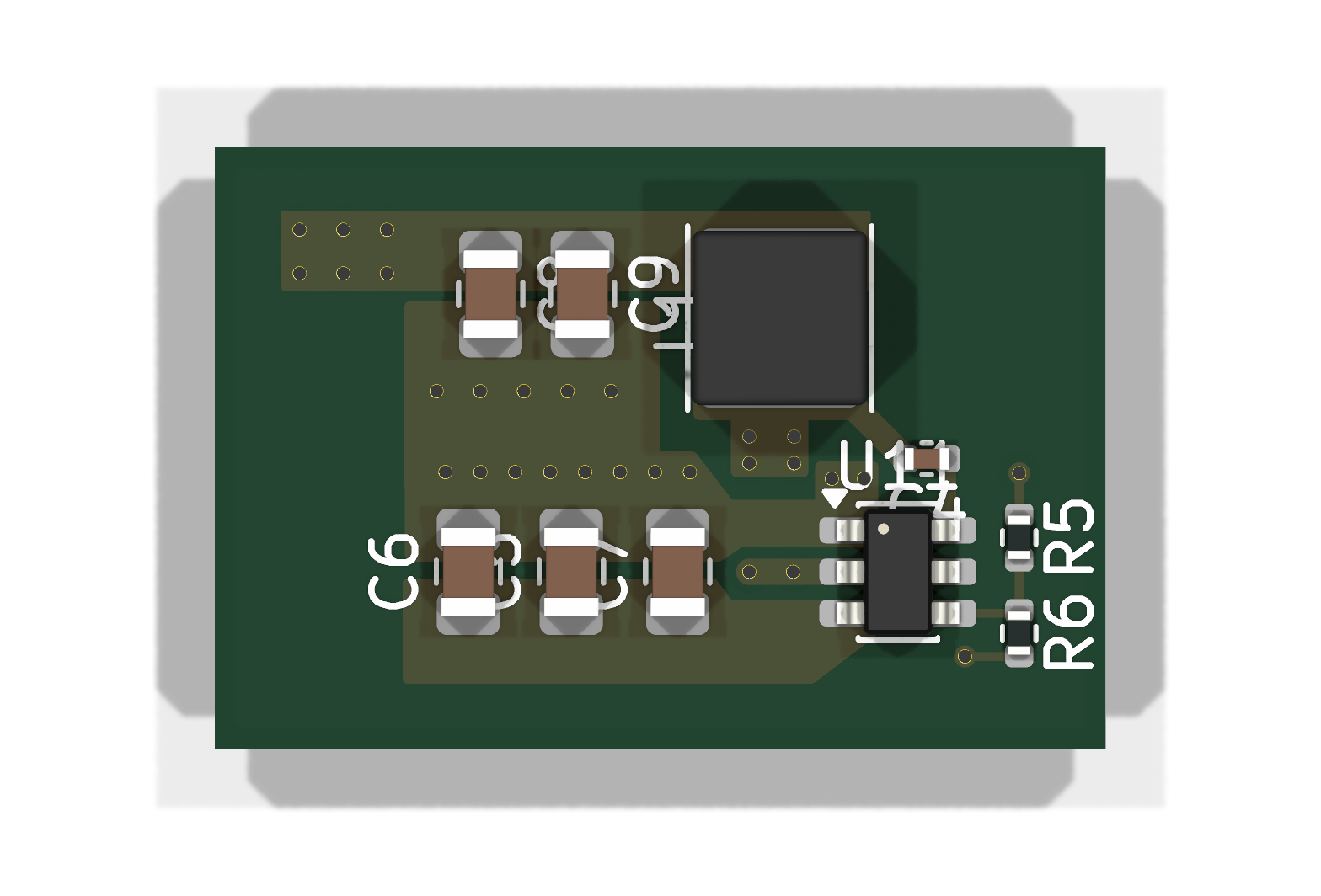
| File | What it is |
|---|---|
TPS563201.kicad_pro / .kicad_sch / .kicad_pcb | the project (open the .kicad_pro) |
docs/TPS563201-schematic.pdf | schematic, readable without KiCad |
docs/TPS563201-layout.svg | F.Cu, B.Cu, silkscreen and outline, readable without KiCad |
docs/webench/ | TI WEBENCH exports the part values came from (BOM CSV, layout images) |
sym/Block.kicad_sym | project-local symbols, so the project opens on any machine |
| Value | |
|---|---|
| Input | 4.75–5.25 V, USB-C VBUS (the connector is outside this block) |
| Output | 3.32 V (0.768 V × (1 + 33.2 k / 10.0 k)) |
| Design current | 1 A (expected load: about 100 mA average, about 570 mA peak) |
| Switching frequency | 580 kHz (TPS563201, D-CAP2, Eco-mode at light load) |
| Main loads on 3.3 V | MCU radio bursts, SCD41 CO₂ sensor (asks for a low-noise supply) |
| Ref | Part | Value | LCSC |
|---|---|---|---|
| U11 | TI TPS563201DDCR, SOT-23-6 | C116592 | |
| L1 | Sunlord SWPA4030S3R3MT, 4 × 4 × 3 mm | 3.3 µH, Isat 3.6 A, DCR 52 mΩ | C15269 |
| C5, C6 | Samsung CL21A106KAYNNNE, 0805 | 10 µF 25 V X5R (input) | C15850 |
| C7 | 0805 | 100 nF (input, high-frequency) | |
| C8, C9 | Samsung CL21A226MAQNNNE, 0805 | 22 µF 25 V X5R (output) | C45783 |
| C4 | Samsung CL05B104KO5NNNC, 0402 | 100 nF (bootstrap) | C1525 |
| R5, R6 | 0402, 1 % | 33.2 k / 10.0 k (feedback) |
TPS563201.kicad_dru).Not fabricated, not measured. The schematic passes ERC (one warning: the +5V net has both a power symbol and a label, as in the full board). The PCB passes DRC with 0 errors, 0 unconnected items and 0 schematic/PCB mismatches.
This project is generated from MultiSensors with
kicad/_generators/export_tps563201_block.py <this folder>. The script takes values,
footprints and MPN/LCSC fields from the MultiSensors schematic, and the layout from
the user's hand-drawn U11 group in the MultiSensors board. Change the block in
MultiSensors and re-export; edits made only here are lost at the next export.
| Qty | Value | Footprint | References |
|---|---|---|---|
| 3 | 4.7uf | Capacitor_SMD:C_1206_3216Metric | C1, C2, C3 |
| 2 | 330mv 1.1A | Diode_SMD:D_SMA | D1, D8 |
| 2 | Polyfuse | Fuse:Fuse_1206_3216Metric | F7, F8 |
| 1 | 0.01uf | Resistor_SMD:R_0805_2012Metric | Cboot1 |
| 1 | 10kOhm | Resistor_SMD:R_0201_0603Metric | R1 |
| 1 | 150uf | Capacitor_Tantalum_SMD:CP_EIA-7343-31_Kemet-D | C4 |
| 1 | 2.87kΩ | Resistor_SMD:R_0402_1005Metric | R2 |
| 1 | 47uh | Inductor_SMD:L_7.3x7.3_H4.5 | L1 |
| 1 | Conn_01x03_Pin | Connector_PinHeader_2.54mm:PinHeader_1x03_P2.54mm_Vertical | J12 |
| 1 | Screw_Terminal_01x02 | TerminalBlock_Ningbo-Kagnex:TerminalBlock_Ningbo-Kagnex_HB9500M_1x02_P9.5mm | J11 |
| 1 | TPS5430DDA | Package_SO:TI_SO-PowerPAD-8_ThermalVias | U3 |
ludodefgh/KicadDesignBlocks
Reusable KiCad circuit blocks (schematic + layout), one self-contained project per block

doudar/SmartSpin2k
Transform your spin bike into a Smart Trainer!

Alia5/PiCCANTE
PiCCANTE is a powerful tool for exploring and reversing CAN busses of vehicles, based on Raspberry Pi Pico (any model)


pms67/BananaSchplit
Single rail DC (<12V) to split rail DC supply (+/-12V and +5V).

intechstudio/knot
Knot is the bridge between old-school MIDI gear like synthesizers, groove boxes, guitar pedals and neat USB MIDI devices.

CuriousMotor/Onyx-Stepper-Motherboard
The successor of the iconic Arduino-CNC-shield

JohnDecebal/UNDR
UNDR AUTO is a fully automatic WDT (Weiss Distribution Technique) tool designed for espresso enthusiasts. This open-source DIY project combines 3D printed parts with electronic and mechanical components to create a…

luftaquila/monolith
DIY wireless real-time datalogging platform for Student Formula and Baja.
It measures 61 × 28 mm and has 2 copper layers, 1.6 mm thick.
15 parts, built around the TPS5430DDA. The full list of its parts is on this page, with links to each part's symbol and footprint where PCBKit's library has them.
From the ludodefgh/KicadDesignBlocks repository on GitHub, at the commit this page was made from: the board is TPS5430Buck/TPS5430Buck.kicad_pcb and its schematic TPS5430Buck/TPS5430Buck.kicad_sch. PCBKit opens the board in the browser, with nothing to install.
Its repository states no licence, so its author keeps all rights: ask ludodefgh before reusing the design.