4 layers90 × 90 mm

 luantty2/Helix-Daughterboard2
Helix daughterboard docs.
Helix Daughterboard is an open-source printed circuit board by luantty2, from the luantty2/Helix-Daughterboard repository on GitHub, published under the MIT licence. It is a 2-layer board of 22.4 × 18.5 mm with 13 parts on 20 nets, routed with 126 tracks and 10 vias.
It is built around the NCP361SN, TPD4E05U06DQAR and SM04B-SRSS-TB, with the U262-241N-4BV60 among its other parts. Its parts include 3 capacitors, 3 resistors, 3 ICs and 2 connectors. It belongs with the keyboards and input and interfaces and adapters boards of this library.


The helix daughterboard is a USB breakout board designed specifically for keyboards. The board integrates 11 components in a relatively small-sized PCB, and it's able to provide full protection for USB2.0 interface.
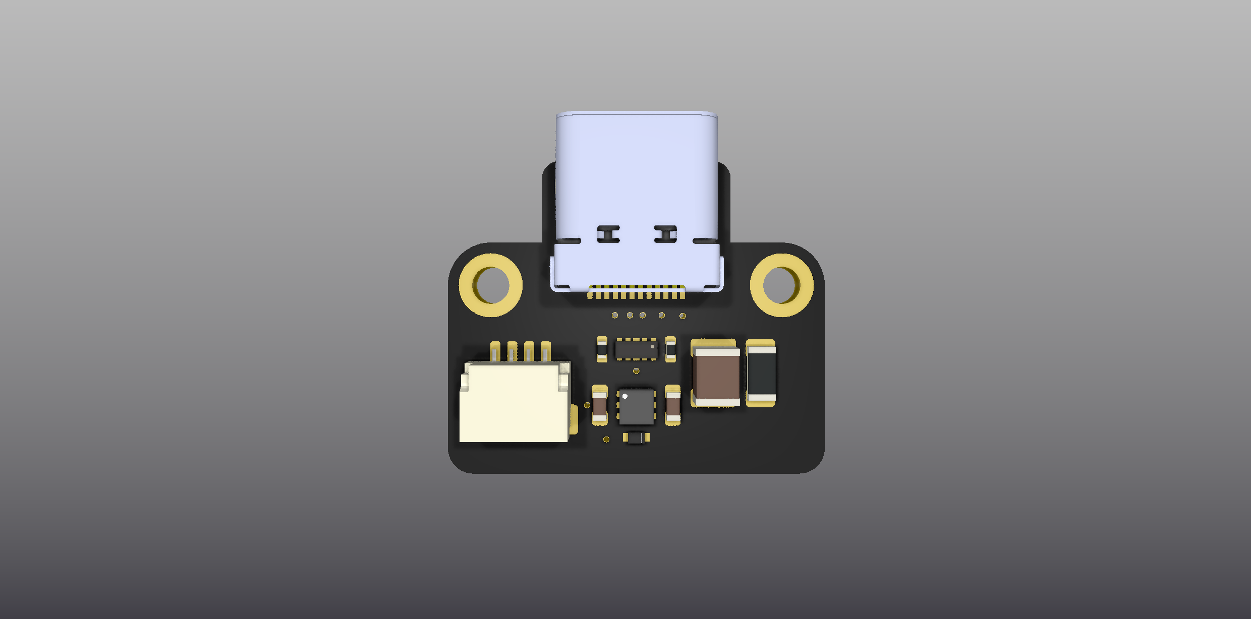
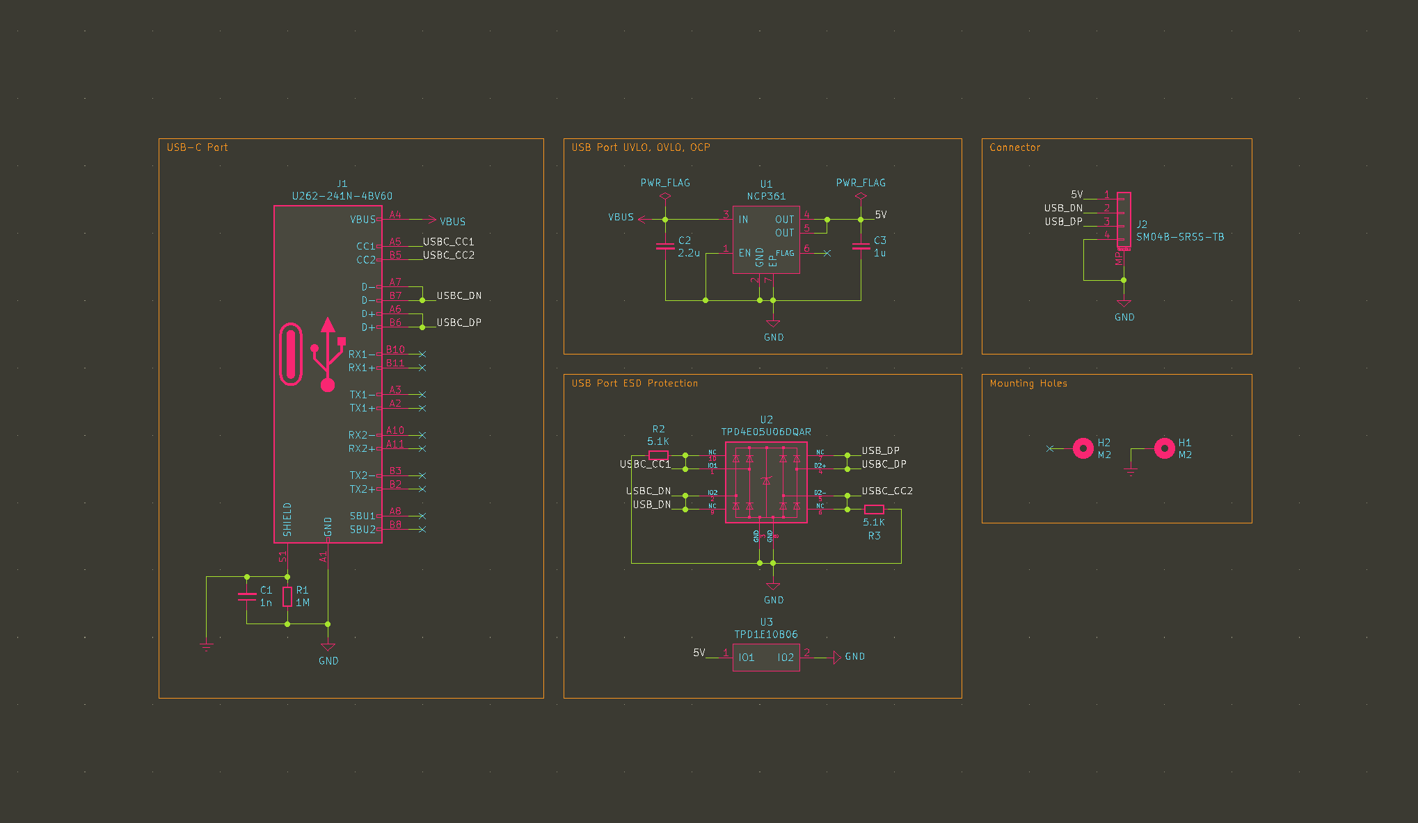
J1 is the USB3.0 receptacle with a row of through-hole data pins, with which the receptacle can be soldered much more firmly. In addition, C1 must have the rated voltage ≥2KV.
U1 is the ONsemi NCP361, which is a single-chip solution for Undervoltage Lockout(UVLO), Overvoltage Lockout(OVLO) and Overcurrent Protection(OCP).
The overvoltage lockout threshold is typically 5.675V and overcurrent limit is internally set to 750mA.
The NCP361 itself complies to IEC61000−4−2 (Level 4), so place the device before U3 to keep VBUS voltage not violating TPD1E10B06's DC breakdown voltage(±6V).
U2 is TPD4E05U06 ESD and surge protection chip for USB data lines and CC pins.
U3 is TPD1E10B06 ESD and surge protection chip for VBUS power.
H1 and H2 are screw mounting holes, one of them is connected to USB shield.
| Designator | Comment | Package | LCSC PN |
|---|---|---|---|
| C1 | 1nF | 1210 | C173219 |
| C2 | 2.2uF | 0603 | C342993 |
| C3 | 1uF | 0603 | C76619 |
| J2 | SM04B-SRSS-TB | - | C160404 |
| R1 | 1M | 1206 | C205050 |
| R2, R3 | 5.1K | 0402 | C203181 |
| U1 | NCP361 | UDFN-6 | C233713 |
| U2 | TPD4E05U06DQAR | USON-10 | C138714 |
| U3 | TPD1E10B06 | X1SON-2 | C48260 |
| J1 | U262-241N-4BV60 | - | C388659 |
| Qty | Value | Footprint | References |
|---|---|---|---|
| 2 | 5.1K | Resistor_SMD:R_0402_1005Metric | R2, R3 |
| 2 | M2 | MountingHole:MountingHole_2.2mm_M2_DIN965_Pad | H1, H2 |
| 1 | 1M | Resistor_SMD:R_1206_3216Metric | R1 |
| 1 | 1n | Capacitor_SMD:C_1210_3225Metric | C1 |
| 1 | 1u | Capacitor_SMD:C_0603_1608Metric | C3 |
| 1 | 2.2u | Capacitor_SMD:C_0603_1608Metric | C2 |
| 1 | NCP361 | digikey-footprints:UDFN-6-1EP_2x2mm | U1 |
| 1 | SM04B-SRSS-TB | Connector_JST:JST_SH_SM04B-SRSS-TB_1x04-1MP_P1.00mm_Horizontal | J2 |
| 1 | TPD1E10B06 | nrfmicro:X1SON-2 | U3 |
| 1 | TPD4E05U06DQAR | Package_SON:USON-10_2.5x1.0mm_P0.5mm | U2 |
| 1 | U262-241N-4BV60 | nrfmicro:USB3_C_Receptacle_HRO | J1 |


nguyencanhanh/luckfox-rv1103-drone
AI quadcopter on one RV1103 (Luckfox Pico Mini B): Linux + RISC-V MCU flight loop, SITL with 3D pilot view, KiCad flight-controller board
It measures 22.4 × 18.5 mm and has 2 copper layers, 1.6 mm thick.
13 parts, built around the NCP361SN, TPD4E05U06DQAR, SM04B-SRSS-TB and U262-241N-4BV60. The full list of its parts is on this page, with links to each part's symbol and footprint where PCBKit's library has them.
From the luantty2/Helix-Daughterboard repository on GitHub, at the commit this page was made from: the board is Hardware/Helix-Daughterboard/Helix-Daughterboard.kicad_pcb. PCBKit opens the board in the browser, with nothing to install.
Its repository publishes it under the MIT licence: you may reuse it on that licence's terms (keep the author's notice, and for a copyleft licence share your changes alike).