2 layers203 × 26.6 mm

 louisquantran/Vector-CPU-Tape-out
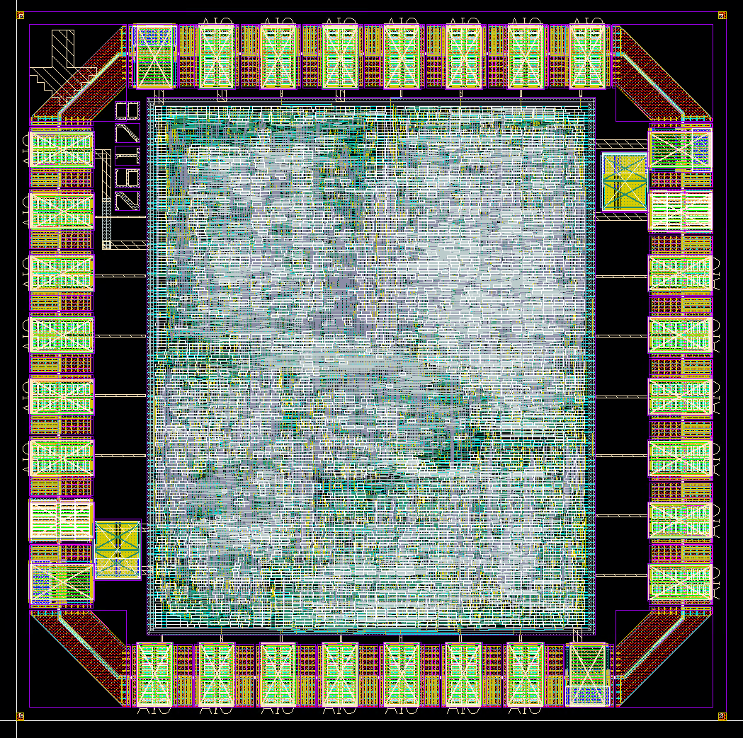
A single-cycle RISC-V CPU with a small subset of the RISC-V Vector (RVV) extension. It was designed in SystemVerilog and taken from RTL to GDS for a 180 nm tape-out in UCLA EE209AS (2026).
Vector CPU is an open-source printed circuit board by louisquantran, from the louisquantran/Vector-CPU-Tape-out repository on GitHub. It is a 2-layer board of 70 × 70 mm with 54 parts on 40 nets, routed with 247 tracks and 2,463 vias.
Its parts include 28 resistors, 17 connectors, 4 capacitors and 1 IC.
A single-cycle RISC-V CPU with a small subset of the RISC-V Vector (RVV) extension. It was designed in SystemVerilog and taken from RTL to GDS for a 180 nm tape-out in UCLA EE209AS (2026).
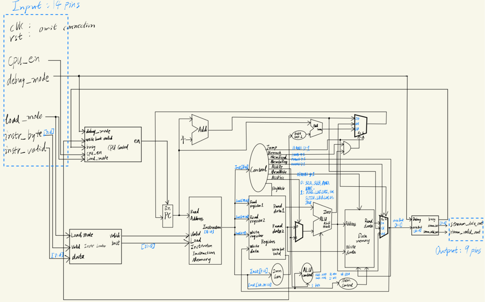
The core runs a subset of RV32I plus vsetvli, unit-stride 32-bit vector loads and stores, and four vector ALU ops on a 4-lane, 128-bit SIMD datapath. The chip has only 23 signal pins, so programs are loaded one byte at a time over an 8-bit port. A debug mode streams every write-back result out over an 8-bit output bus.
| Folder | Contents |
|---|---|
Vector_CPU/ | Taped-out design. Scalar core + vector unit (rtl/), testbenches (tb/), Hammer configs (design/), chip-testing PCB (PCB/) |
CPU/ | Earlier scalar-only version of the same core (no vector unit) |
SIMD_ALU/ | First block: a combinational 16-bit SIMD ALU (2 × 8-bit lanes: ADD, AND, OR, SHIFT) |
docs/ | Datapath diagram and final layout screenshot |
v0–v3), unmasked instructions onlysimd_alu_4lane: four 32-bit lanes in parallel, with tail-undisturbed or tail-agnostic handling (the agnostic tail is written with all 1s)chip_top): 32-word instruction memory, 64-byte data memory.| Class | Instructions |
|---|---|
| Scalar (RV32I subset) | LUI, ADDI, ORI, SLTIU, SUB, AND, SRA, LW, LBU, SW, SH, BNE, JALR |
| Vector config | vsetvli (only e32, m1; vl = min(AVL, 4), including the rs1 = x0 special cases) |
| Vector memory | vle32.v, vse32.v (unit-stride) |
| Vector ALU | vadd.vv, vsub.vv, vand.vv, vor.vv |
14 inputs, 9 outputs, plus VDD and VSS. Everything runs on one clock (clk, with a 10 ns / 100 MHz target).
| Pin | Dir | Description |
|---|---|---|
clk, rst | in | Clock and asynchronous active-high reset |
load_mode | in | High: program-load mode (also holds the core in reset) |
instr_byte_in[7:0] | in | Program bytes during load mode |
instr_byte_valid | in | Qualifies instr_byte_in |
cpu_en | in | Run enable |
debug_stream_mode | in | Stream every write-back result to the output port |
stream_data_out[7:0] | out | Streamed result bytes |
stream_valid_out | out | Qualifies stream_data_out |
rst.load_mode. For each 32-bit instruction, send 4 bytes least-significant byte first, holding instr_byte_valid high for one clock per byte. Words are written in order starting at address 0.load_mode and raise cpu_en. Execution starts at PC 0.debug_stream_mode high, each result the core writes back goes out as 4 bytes, LSB first, with stream_valid_out high. Results come from scalar rd writes, the new vl from vsetvli, each vector-load element, and each lane of a SIMD result. The core stalls while it streams, so no results are lost. With debug_stream_mode low, the core runs at full speed and nothing is streamed.The testbenches in Vector_CPU/tb/ check themselves. They load a program through the byte port, step through it checking the scalar and vector registers, then check that the debug output stream matches the expected sequence of words.
| Testbench | Coverage |
|---|---|
core_tb.sv | Full 79-instruction regression with branch and loop scenarios (needs IMEM_WORDS = 128) |
core_tb_short.sv | Fits a 32-word IMEM: LUI, ADDI, AND, SW, LW, JALR, BNE + vector ops |
core_tb_short2.sv | Fits a 32-word IMEM: ORI, SLTIU, SUB, SRA, SH, LBU + all vector ops at vl = 4 (used for gate-level sim) |
The design was implemented with Hammer driving Cadence Genus (synthesis), Innovus (place and route), Tempus (STA) and Conformal (equivalence), Mentor Calibre (DRC/LVS), and Synopsys VCS (RTL and gate-level simulation).
design/design.yml: top module, RTL file list, clock and I/O constraints, a 600 × 720 µm floorplan, pin placement and the power-ring/strap scriptdesign/tb.yml: simulation setup for RTL, post-synthesis and post-PAR runsNote on the PDK: the process design kit is under NDA. In the published
design.ymlfiles, process-specific values (technology, node, cell names, metal layer names and design-rule values) are replaced with<placeholders>. Fill these in from your own PDK before running Hammer. Hammer's own configs (env.ymland the tech plugin) are not included.The
input_filespaths in the configs (../ECE209/...) are relative to the original Hammer run directory. Update them to point atVector_CPU/rtl/andVector_CPU/tb/in this repo.
Vector_CPU/PCB/ has the KiCad project for the chip-testing PCB: schematic, board layout, and the chip's symbol and footprint.
| Qty | Value | Footprint | References |
|---|---|---|---|
| 28 | 1K | Resistor_SMD:R_0805_2012Metric_Pad1.20x1.40mm_HandSolder | R11, R12, R13, R14, R19, R20, R21, R22, R23, R24, R25, R26, R27, R28, R29, R30 +12 |
| 12 | Conn_02x03_Odd_Even | Connector_PinHeader_2.54mm:PinHeader_2x03_P2.54mm_Vertical | J5, J14, J15, J16, J17, J18, J19, J20, J21, J22, J23, J24 |
| 5 | Conn_02x02_Odd_Even | Connector_PinHeader_2.54mm:PinHeader_2x02_P2.54mm_Vertical | J9, J25, J26, J27, J28 |
| 4 | , , , | ||
| 1 | 0.22u | Capacitor_SMD:C_0805_2012Metric_Pad1.18x1.45mm_HandSolder | C17 |
| 1 | 2.2n | Capacitor_SMD:C_0805_2012Metric_Pad1.18x1.45mm_HandSolder | C16 |
| 1 | 22p | Capacitor_SMD:C_0805_2012Metric_Pad1.18x1.45mm_HandSolder | C15 |
| 1 | 22u | Capacitor_SMD:C_0805_2012Metric_Pad1.18x1.45mm_HandSolder | C18 |
| 1 | ~ | EE209AS_2026:EE209AS_2026 | U2 |
It measures 70 × 70 mm and has 2 copper layers, 1.6 mm thick.
54 parts. The full list of its parts is on this page, with links to each part's symbol and footprint where PCBKit's library has them.
From the louisquantran/Vector-CPU-Tape-out repository on GitHub, at the commit this page was made from: the board is Vector_CPU/PCB/PCB.kicad_pcb and its schematic Vector_CPU/PCB/PCB.kicad_sch. PCBKit opens the board in the browser, with nothing to install.
Its repository states no licence, so its author keeps all rights: ask louisquantran before reusing the design.


MaltWhiskey/Mega-Cube
16x16x16 PL9823 Cube with Teensy 4.0 and FlexIO driver


brickbots/PiFinder
A plate solving telescope finder based around a Raspberry PI and RPI HQ Camera