
2 layers110.7 × 67.8 mm
Cyberdeck
awesomebrownies/cyberdeck
Deck Featuring: Controllers, shock cage, folding travel mode, and picatinny rails
38 parts2
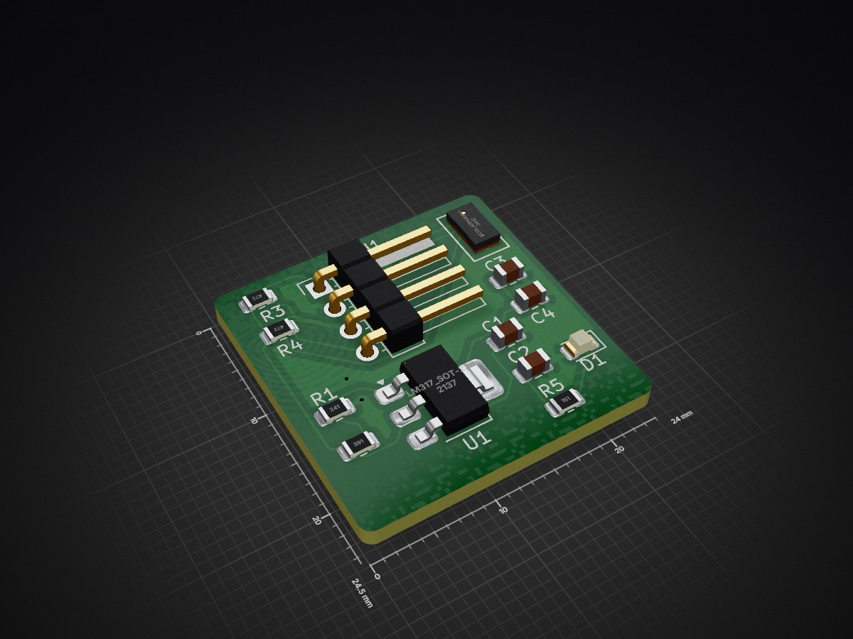
 liziying115-dev/PCB_Design_Lab
PCB Design Lab is an open-source printed circuit board by liziying115-dev, from the liziying115-dev/PCB_Design_Lab repository on GitHub. It is a 2-layer board of 24 × 24.5 mm with 13 parts on 9 nets, routed with 75 tracks and 2 vias.
It is built around the VL53L4CDV0DH/1. Its parts include 5 resistors, 4 capacitors, 2 ICs, 1 diode and 1 connector.
| Qty | Value | Footprint | References |
|---|---|---|---|
| 2 | 0.1µF | Capacitor_SMD:C_0805_2012Metric | C1, C4 |
| 2 | 4.7kΩ | Resistor_SMD:R_0805_2012Metric | R3, R4 |
| 1 | 10µF | Capacitor_SMD:C_0805_2012Metric | C2 |
| 1 | 150Ω | Resistor_SMD:R_0805_2012Metric | R5 |
| 1 | 240Ω | Resistor_SMD:R_0805_2012Metric | R1 |
| 1 | 390Ω | Resistor_SMD:R_0805_2012Metric | R2 |
| 1 | 4.7µF | Capacitor_SMD:C_0805_2012Metric | C3 |
| 1 | Conn_01x04_Pin | Connector_PinHeader_2.54mm:PinHeader_1x04_P2.54mm_Horizontal | J1 |
| 1 | LED | LED_SMD:LED_0805_2012Metric | D1 |
| 1 | LM317_SOT-223 | Package_TO_SOT_SMD:SOT-223-3_TabPin2 | U1 |
| 1 | VL53L4CDV0DH/1 | ul_VL53L4CDV0DH-1:LGA12_STM | U3 |
awesomebrownies/cyberdeck
Deck Featuring: Controllers, shock cage, folding travel mode, and picatinny rails

open-thngs/trap-a-rep-trigger
Device to detect passing creatures to trigger an external device like a DSLR camera

oddgrd/auge
This repo contains the kicad PCB files, as well as libraries for footprints and symbols, for my [VL53L4CD][https://www.st.com/en/imaging-and-photonics-solutions/vl53l4cd.html] daughterboard.


samyk/magspoof
A portable device that can spoof/emulate any magnetic stripe, credit card or hotel card "wirelessly", even on standard magstripe (non-NFC/RFID) readers.
It measures 24 × 24.5 mm and has 2 copper layers, 1.6 mm thick.
13 parts, built around the VL53L4CDV0DH/1. The full list of its parts is on this page, with links to each part's symbol and footprint where PCBKit's library has them.
From the liziying115-dev/PCB_Design_Lab repository on GitHub, at the commit this page was made from: the board is PCB Design Lab.kicad_pcb and its schematic PCB Design Lab.kicad_sch. PCBKit opens the board in the browser, with nothing to install.
Its repository states no licence, so its author keeps all rights: ask liziying115-dev before reusing the design.