4 layers70 × 65 mm
ESP32 FC
JS2028EE/ESP32_FC
This is the current editable KiCad 10 project for a 70 x 65 mm, four-layer controller, with an ESP32-S3-WROOM-1-N8R8, BMI088 SPI IMU, BMP280 barometer and a separate 4-in-1 ESC.
107 parts
 lindestad/wind-controller
LINDESTAD simracing wind controller: ESP32-C3 Zephyr firmware, KiCad PCB and SimHub integration
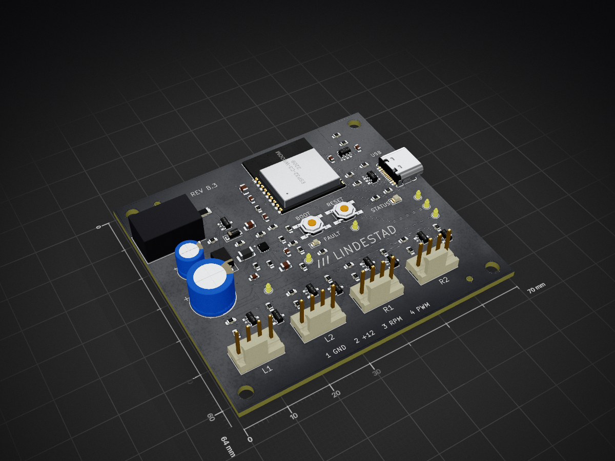
Windpcb is an open-source printed circuit board by lindestad, from the lindestad/wind-controller repository on GitHub. It is a 2-layer board of 70 × 64 mm with 82 parts on 55 nets, routed with 629 tracks and 104 vias.
It is built around the ESP32-C3-WROOM-02-N4, AP2112K-3.3TRG1 and USBLC6-2SC6, with the SI2312-TP, CC0603KRX7R9BB104 and CL21B105KBFNNNE among its other parts. Its parts include 32 resistors, 11 capacitors, 9 transistors, 6 connectors and 4 ICs. It belongs with the ESP32 and RISC-V boards of this library.


70 × 64 mm, black solder mask, white silkscreen, two-layer 1.6 mm FR-4 / 1 oz copper. ESP32-C3-WROOM-02-N4; four ARCTIC P14 Pro PST headers; native USB-C; protected 12 V input.
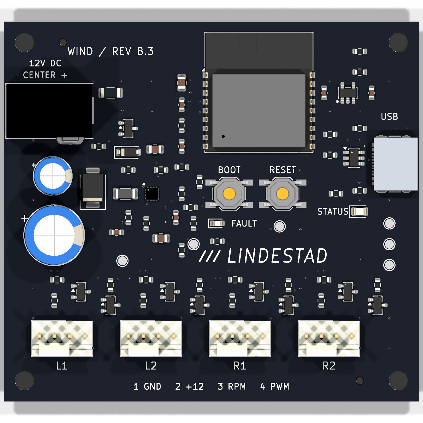
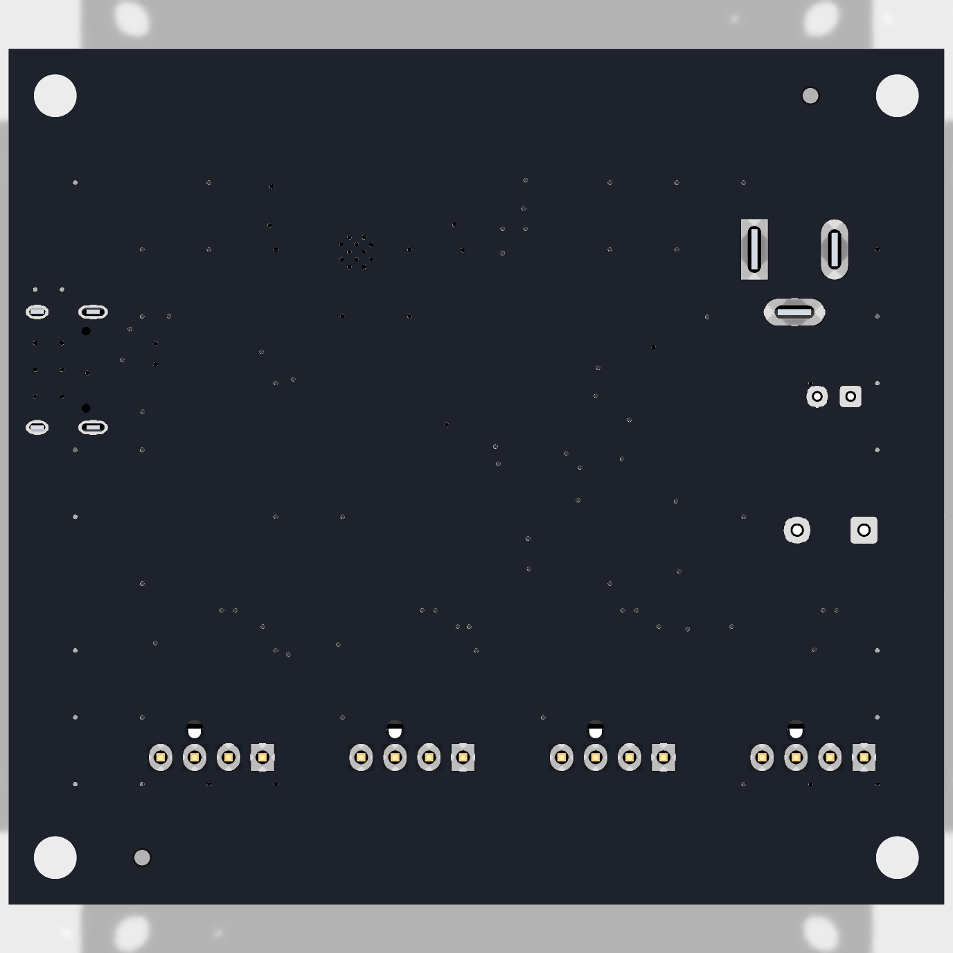
These are CAD renders, not photographs. J1, J2 and U4 have representative visual bodies; their manufacturer drawings and electrical pads govern assembly.
windpcb.kicad_pro. All project-specific symbols, footprints and visual models
are under libraries/; library tables use ${KIPRJMOD}. Standard STEP models use
${KICAD10_3DMODEL_DIR}. No files from the author's KiCad folder are needed.J1 takes a 5.5 × 2.5 mm centre-positive 12 V barrel plug. Use a regulated supply with sufficient startup margin (at least 3 A recommended). Each fan has its own header; leave PST daisy-chain sockets unused. Pin order: 1 GND, 2 +12 V, 3 tach, 4 PWM.
The included CPL is the original submitted file, with explicit connector/capacitor insertion-origin offsets. JLC subsequently corrected several component orientations in its own assembly system. The final numeric machine placement file was not supplied. This release therefore requires a fresh supplier placement review; uploading the CPL alone does not reproduce that approval. Verify every polarized part/pin 1 against the native CAD and assembly drawing, especially Q1–Q9, U2/U3/U4, J2–J6, D1–D4 and C6/C9. The first assembled board has since operated successfully with the firmware.
U4 TPS25970LRPWR has ten electrical terminals, even when a supplier's generic visual model shows sixteen leads. Its 16 split paste apertures are intentional. Preserve the TI-derived RPW0010A lands and 0.100 mm stencil prescription; ask the assembler to review the eFuse, USB-C, and ESP32 thermal-via soldering process for its selected finish.
H1–H4: 3.2 mm M3 mounting holes, 63 × 57 mm spacing. H5/H6 are 1.152 mm NPTH tooling holes with 0.148 mm mask expansion. Their centres are (10, 3.5) and (60, 60.5) mm from the upper-left corner. The CPL origin is the lower-left corner; X right, Y up.
Run the exporter with KiCad's Python (which provides pcbnew). On Windows:
& 'C:/Program Files/KiCad/10.0/bin/python.exe' -m pip install --target hardware/tools/vendor -r hardware/tools/requirements.txt
& 'C:/Program Files/KiCad/10.0/bin/python.exe' hardware/tools/export.py
On another installation, put kicad-cli on PATH or set KICAD_CLI and use a Python
environment that can import KiCad 10's pcbnew. The exporter runs ERC, full DRC with
schematic parity, checks every pad/net, exports manufacturing files/BOM/CPL, PDFs,
board-only STEP, pictures and SHA256 hashes. It does not rebuild or reroute the PCB.
Historical one-time layout generators were deliberately not included as build steps.
Engineering specifications and revision notes are in docs/. Their pre-order wording
and references to historical local reports describe earlier reviews, not the current
hardware test status. The root README and docs/validation.md describe current tests.
Private supplier order/account records are not part of this public release.
Sources: TI TPS2597, ARCTIC P14 Pro PST, JLC tooling guide.
| Qty | Value | Footprint | References |
|---|---|---|---|
| 8 | SI2312-TP | Wind:Package_TO_SOT_SMD_SOT-23 | Q2, Q3, Q4, Q5, Q6, Q7, Q8, Q9 |
| 6 | 10k | Wind:Resistor_SMD_R_0603_1608Metric | R5, R6, R7, R8, R15, R17 |
| 5 | 100 | Wind:Resistor_SMD_R_0603_1608Metric | R20, R25, R30, R35, R40 |
| 5 | 2.2k | Wind:Resistor_SMD_R_0603_1608Metric | R18, R22, R27, R32, R37 |
| 4 | 100k | Wind:Resistor_SMD_R_0603_1608Metric | R21, R26, R31, R36 |
| 4 | M3 | MountingHole_3.2mm_M3 | H1, H2, H3, H4 |
| 3 | 100nF / 50V | Wind:Capacitor_SMD_C_0603_1608Metric | C4, C8, C11 |
| 3 | 1k | Wind:Resistor_SMD_R_0603_1608Metric | R9, R14, R19 |
| 3 | 1uF / 50V | Wind:Capacitor_SMD_C_0603_1608Metric | C1, C2, C5 |
| 2 | 1uF / 50V | Wind:Capacitor_SMD_C_0805_2012Metric | C7, C10 |
| 2 | 22 | Wind:Resistor_SMD_R_0603_1608Metric | R3, R4 |
| 2 | 4.7k | Wind:Resistor_SMD_R_0603_1608Metric | R10, R16 |
| 2 | 5.1k | Wind:Resistor_SMD_R_0603_1608Metric | R1, R2 |
| 2 | JLC TOOL 1.152 NPTH | Wind:JLC_Tooling_1.152 | H5, H6 |
| 1 | +3V3 | Wind:TestPoint_TestPoint_Pad_D1.5mm | TP2 |
| 1 | 10k 0.1% | Wind:Resistor_SMD_R_0603_1608Metric | R12 |
| 1 | 10uF / 50V | Wind:Capacitor_SMD_C_0805_2012Metric | C3 |
| 1 | 120R@100MHz / 3.5A | Wind:Inductor_SMD_L_1206_3216Metric | FB1 |
| 1 | 12V / CENTER + | Wind:BarrelJack_XKB_DC-005-5A-2.5 | J1 |
| 1 | 2.4k 1% | Wind:Resistor_SMD_R_0603_1608Metric | R13 |
| 1 | 3A / 32V | Wind:Fuse_Fuse_1206_3216Metric | F1 |
| 1 | 470uF / 25V | Wind:Capacitor_THT_CP_Radial_D10.0mm_P5.00mm | C9 |
| 1 | 47uF / 50V | Wind:Capacitor_THT_CP_Radial_D6.3mm_P2.50mm | C6 |
| 1 | 97.6k 0.1% | Wind:Resistor_SMD_R_0603_1608Metric | R11 |
| 1 | AO3401A | Wind:Package_TO_SOT_SMD_SOT-23 | Q1 |
| 1 | AP2112K-3.3 | Wind:Package_TO_SOT_SMD_SOT-23-5 | U2 |
| 1 | BOOT | Wind:Button_Switch_SMD_SW_SPST_TL3342 | SW1 |
| 1 | BZT52C9V1 | Wind:Diode_SMD_D_SOD-123 | D1 |
| 1 | EFUSE_EN | Wind:TestPoint_TestPoint_Pad_D1.5mm | TP6 |
| 1 | ESP32-C3-WROOM-02-N4 | Wind:RF_Module_ESP32-C3-WROOM-02 | U1 |
| 1 | FAN_12V | Wind:TestPoint_TestPoint_Pad_D1.5mm | TP3 |
| 1 | FAULT RED | Wind:LED_SMD_LED_0603_1608Metric | D4 |
| 1 | FAULT_N | Wind:TestPoint_TestPoint_Pad_D1.5mm | TP5 |
| 1 | GND | Wind:TestPoint_TestPoint_Pad_D1.5mm | TP1 |
| 1 | L1 | Wind:Connector_FanPinHeader_1x04_P2.54mm_Vertical | J3 |
| 1 | L2 | Wind:Connector_FanPinHeader_1x04_P2.54mm_Vertical | J4 |
| 1 | R1 | Wind:Connector_FanPinHeader_1x04_P2.54mm_Vertical | J5 |
| 1 | R2 | Wind:Connector_FanPinHeader_1x04_P2.54mm_Vertical | J6 |
| 1 | RESET | Wind:Button_Switch_SMD_SW_SPST_TL3342 | SW2 |
| 1 | SMBJ15A TVS | Wind:Diode_SMD_D_SMB | D2 |
| 1 | STATUS GREEN | Wind:LED_SMD_LED_0805_2012Metric | D3 |
| 1 | TPS25970LRPWR | Wind:TPS25970_RPW0010A_2x2mm | U4 |
| 1 | USB-C DATA | Wind:Connector_USB_USB_C_Receptacle_HRO_TYPE-C-31-M-12 | J2 |
| 1 | USBLC6-2SC6 | Wind:Package_TO_SOT_SMD_SOT-23-6 | U3 |
| 1 | VIN_FILTERED | Wind:TestPoint_TestPoint_Pad_D1.5mm | TP4 |
It measures 70 × 64 mm and has 2 copper layers, 1.6 mm thick.
82 parts, built around the ESP32-C3-WROOM-02-N4, AP2112K-3.3TRG1, USBLC6-2SC6 and SI2312-TP. The full list of its parts is on this page, with links to each part's symbol and footprint where PCBKit's library has them.
From the lindestad/wind-controller repository on GitHub, at the commit this page was made from: the board is hardware/windpcb.kicad_pcb and its schematic hardware/windpcb.kicad_sch. PCBKit opens the board in the browser, with nothing to install.
Its repository states no licence, so its author keeps all rights: ask lindestad before reusing the design.
JS2028EE/ESP32_FC
This is the current editable KiCad 10 project for a 70 x 65 mm, four-layer controller, with an ESP32-S3-WROOM-1-N8R8, BMI088 SPI IMU, BMP280 barometer and a separate 4-in-1 ESC.

gmaxdragon/Seizo-Noise
A massive PCB for a speaker for my robotic arm with a microphone built into it and a ton of other GPIO ports.


misko/prompt2device
The separate vNext PCB skill and orchestrator package is available alongside the reference workflow below; existing projects keep their accepted toolchain until an explicit migration.

aliaksei-lameyka/ENKU-Base-reader
Open enku-mainboard-r0.1.kicadpro with KiCad10.0.7. Matching PCB/root schematic and power.kicadsch, mcuio.kicadsch, epdhv.kicadsch, connectors.kicadsch are canonical.

AndrewCraswell/agency
Native KiCad engineering prototype, separate from the earlier ESP32/tscircuit board. Open usb-scoring-platform.kicadpro in KiCad 10; schematic and PCB are the editable source, with no generator required.