2 layers44.5 × 46.9 mm
OSO SWAT B1-jig
joeycastillo/Sensor-Watch
A board replacement for the classic Casio F-91W wristwatch
31 parts2.1k
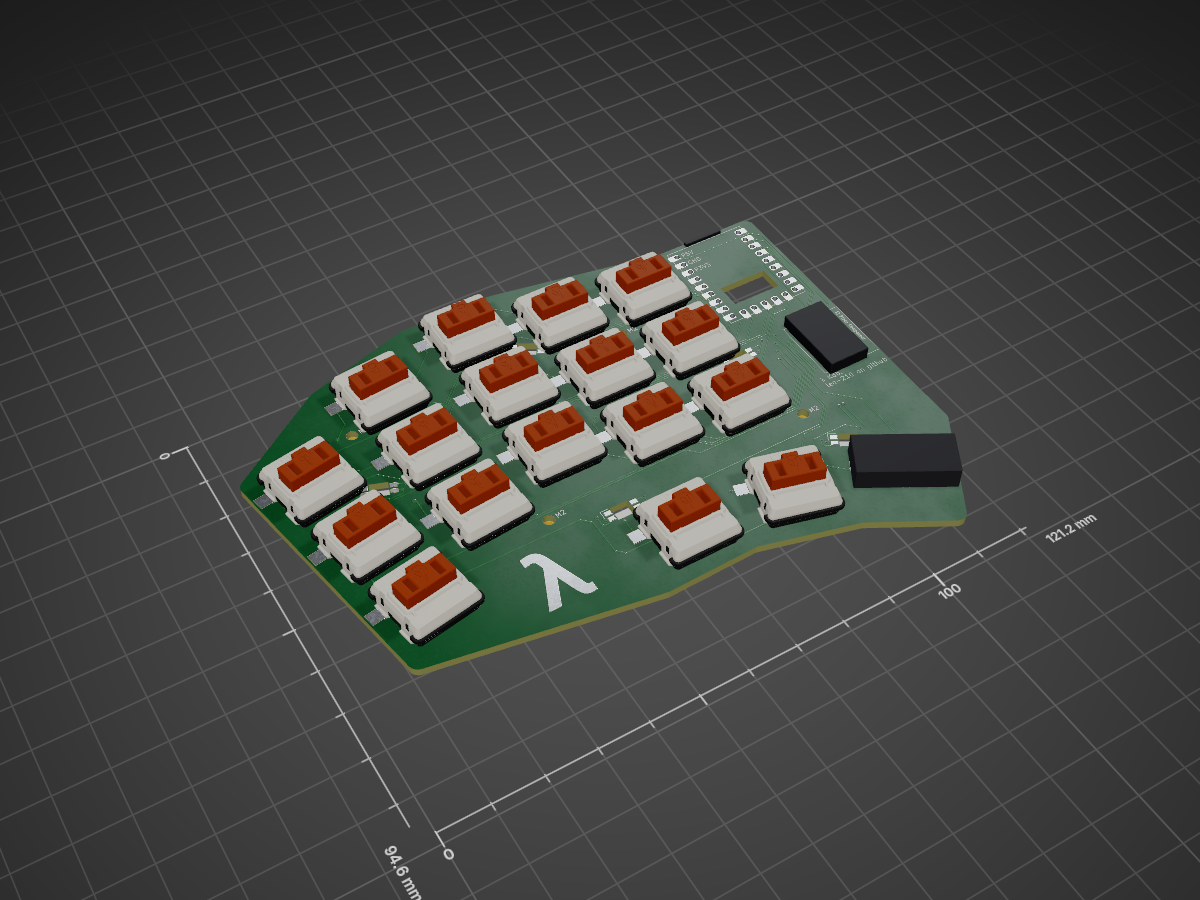
 leo-210/lambda-keyboard1
A custom 36-key wired split keyboard.
Kdb v1 is an open-source printed circuit board by leo-210, from the leo-210/lambda-keyboard repository on GitHub, published under the CC0-1.0 licence. It is a 2-layer board of 121.1 × 94.5 mm with 31 parts on 28 nets, routed with 631 tracks and 66 vias.
Its parts include 18 switches and 5 diodes. It belongs with the keyboards and input boards of this library.
A custom 36-key wired ChocV1 split keyboard.
Note : this keyboard is my first design, and while taking it as an inspiration can be a good idea, please think before building exactly this design : there are a few flaws that I wrote about below.
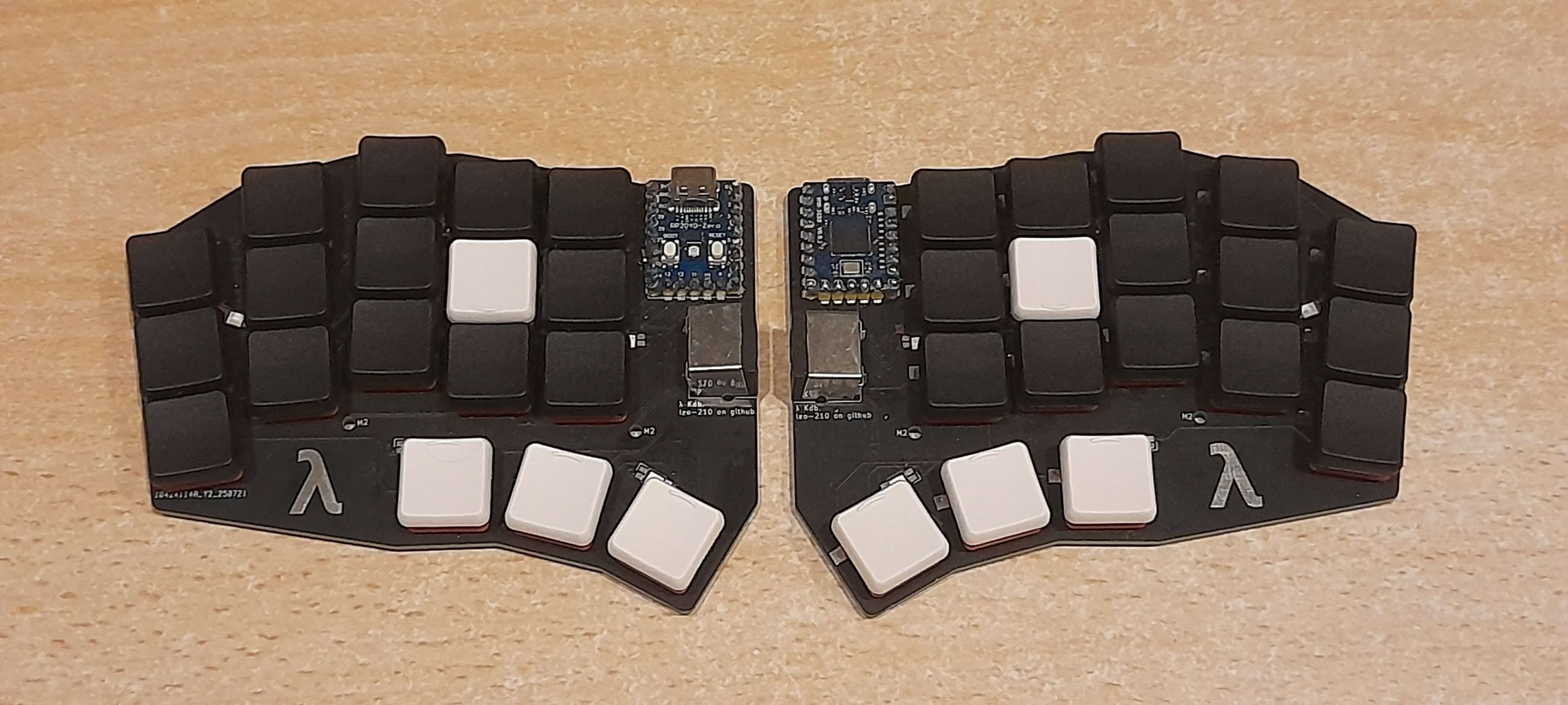
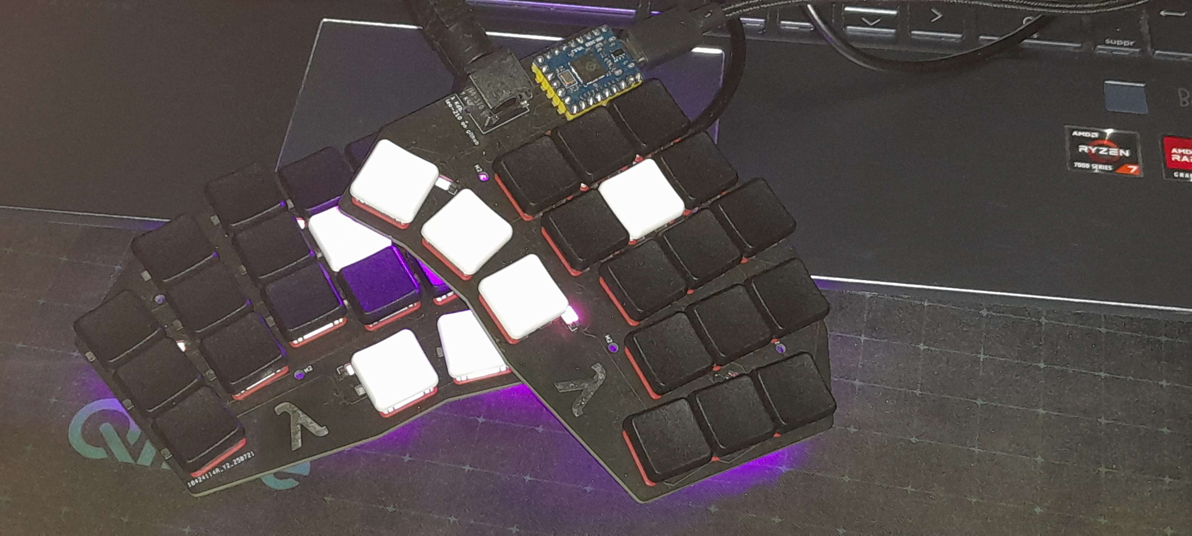
To build the keyboard, you'll need :
The keyboard is diode-less !
You can also design your own case, but I did not bother.
Ordering everything in France, including soldering tools, it cost about 110 €, where approximately a third was for electrical components and the PCB, a second third for key caps and switches, and the last third for shipping costs.
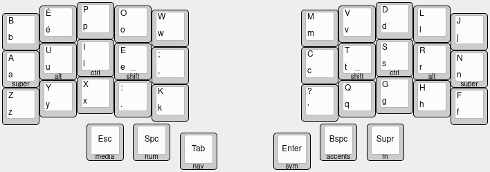
This repo also contains QMK firmware for this keyboard, using the BÉPO french layout. The keyboard layout was inspired by Miryoku, and you can view it on keyboard-layout-editor.com.
I fell into the rabbit hole of custom split keyboards, and with all the summer holidays in front of me, I couldn't hold back. It was a fun project !
I chose to make my own design because none where satisfying all my requirements, which were :
With enough research I maybe could have found something, but designing it myself was far more interesting.
If you want a split keyboard, you can definitely think about creating your own ! It is not as difficult as it would seem, and this journey is well documented and there are a lot of tools to make your life easier.
I like this Greek letter, and my name starts with an L.
As my first design, nothing is perfect, and here are some things I would change for a future design.
I like that the mini DIN protects my keyboard from shorting, but the cable is really bulky. I'll think about changing to USB C next time, or just TRRS, even with the lack of shorting safety.
Writing in English is not a problem, but in french with accents everywhere I find it painful to constantly use layers. It is possible and can even become reliable, but for now I couldn't really get used to it (maybe I haven't used the keyboard enough yet...).
Also, for coding, where a lot of special symbols are needed, a couple more keys could be useful.
Only 5 underglow LEDs are not enough in my opinion, you can see their light but there are some "holes". Also, for a future keyboard I'd like per key lighting as well, even if it requires more work.
Seems fun.
Without this text, JLC PCB wrote a random number in a random place on my PCBs... Fortunately it does not look that bad.
| Qty | Value | Footprint | References |
|---|---|---|---|
| 18 | PG1350 | S1, S2, S3, S4, S5, S6, S7, S10, S11, S12, S13, S14, S15, S16, S17, S18 +2 | |
| 5 | ceoloide:led_SK6812mini-e (underglow, reversible) | LED1, LED2, LED3, LED4, LED5 | |
| 4 | ceoloide:mounting_hole_npth | MH1, MH2, MH3, MH4 | |
| 2 | LOGO | footprints:lambda | G***, G*** |
| 1 | RP2040-Zero | RP2040Zero1 | |
| 1 | MiniDIN4 | AdamTech_MDJ-004-FS_reversible | AdamTech-MDJ004FS1 |
It measures 121.1 × 94.5 mm and has 2 copper layers, 1.6 mm thick.
31 parts. The full list of its parts is on this page, with links to each part's symbol and footprint where PCBKit's library has them.
From the leo-210/lambda-keyboard repository on GitHub, at the commit this page was made from: the board is pcbs/kdb-v1.kicad_pcb. PCBKit opens the board in the browser, with nothing to install.
Its repository publishes it under the CC0-1.0 licence: you may reuse it on that licence's terms (keep the author's notice, and for a copyleft licence share your changes alike).
joeycastillo/Sensor-Watch
A board replacement for the classic Casio F-91W wristwatch

hoglet67/RGBtoHDMI
Bare-metal Raspberry Pi project that provides pixel-perfect sampling of Retro Computer RGB/YUV video and conversion to HDMI

hackclub/OnBoard
💡 Join 1,000 teenagers and make your first PCB with a $100 grant!

openwch/ch32v003
CH32V003 is an ultra-cheap RISC-V MCU with 2KB SRAM, 16KB flash, and up to 18 GPIOs that sells for under $0.10

Luos-io/luos_engine
Open-source and real-time orchestrator for cyber-physical-systems, to easily design, test and deploy embedded applications and digital twins.

BlueAndi/Pixelix
Full RGB LED matrix, based on an ESP32 and WS2812B LEDs or emulated LEDs on TFT.

