4 layers
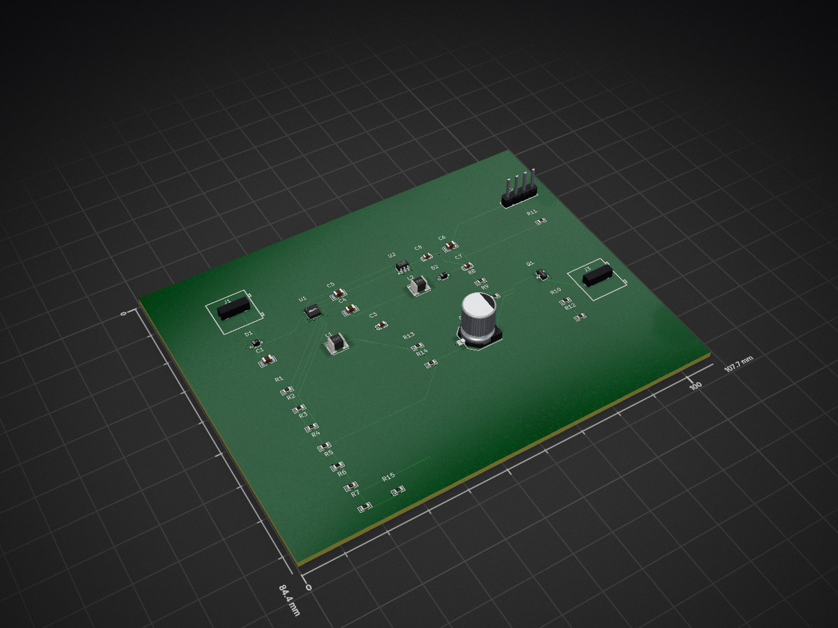
 Lazztech/TEG
Electronics for a thermal energy harvesting prototype: a small TEG array feeds a sub-1 V energy-harvesting front-end (BQ25504), which charges a buffer capacitor and backs up a regulated 5 V rail for a Noctua 5 V PWM fan…
TEG is an open-source printed circuit board by Lazztech, from the Lazztech/TEG repository on GitHub. It is a 2-layer board of 107.7 × 84.4 mm with 33 parts on 21 nets, routed with 302 tracks and 34 vias.
It is built around the MT3608, 1N5819WS and AO3400A. Its parts include 15 resistors, 8 capacitors, 3 connectors, 2 ICs and 2 diodes.


Electronics for a thermal energy harvesting prototype: a small TEG array feeds a sub-1 V energy-harvesting front-end (BQ25504), which charges a buffer capacitor and backs up a regulated 5 V rail for a Noctua 5 V PWM fan and a test load.
Originally drafted on Flux.ai; this repo is the KiCad continuation, prepared for JLCPCB — made and assembled.
Status: the sub-watt board is complete, routed, DRC-clean and orderable — but it is now a REFERENCE, not the deliverable. REQUIREMENTS.md re-scopes the project to a fireplace-mounted, wedge-shaped harvester producing ~3–4 W with USB-A and USB-C output. At ~3–4 W the BQ25504 (max input power ≤ 300 mW) cannot be used, so a new power board is in design.
Settled — nothing here needs your input.
| Question | Decision | Why |
|---|---|---|
| Storage: battery or supercap? | Neither — a 1000 µF electrolytic buffer (option D) | JLCPCB stocks no supercapacitors and no batteries (verified against their API), so those can't be machine-assembled. An electrolytic keeps the board 100 % JLCPCB-assembled. Trade-off accepted: ≈5 mJ stored, so the fan runs only on live harvest, not from storage |
| MPPT? | Yes — built into the BQ25504 | Sample-and-hold MPPT in hardware; no extra IC, no firmware |
| MPPT ratio | ≈50 % of Voc (R13 = R14 = 10 MΩ) | A TEG makes maximum power at a matched load, ≈50 % of its open-circuit voltage. The datasheet's 78 % default is tuned for solar |
| Voltage window | VBAT_OV 3.15 V (datasheet-verified) | Conservative and tested. Protects the part; tune later if you want more usable energy |
| Charge cutoff | OT_PROG → GND = 65 °C | Sensible protection for a device that is warm by design |
VBAT_OK | Left unconnected (no-connect marker) | With no real energy store, gating the load buys little. Wiring it to the MT3608 EN is the natural upgrade if you later add a supercap |
| # | Task | Notes |
|---|---|---|
| 1 | Done — FreeRouting, 0 DRC violations | |
| 2 | Done — gerbers, drill, position, BOM in build/fab/ (verify CPL rotations) | |
| 3 | Review and order | Read build/fab/TEG-routed.pdf and confirm the layout; then order from JLCPCB. ⚠️ U1 BQ25504RGTT stock is only 7 — C2876746 is the same part if it sells out |
| 4 | Optional: add a GND pour | GND is routed as traces so the board works as-is. A pour is a nice refinement — fill it in KiCad (zones can't be filled from the CLI) |
| 5 | Bench-verify before trusting the TEGs | Drive the input from a bench supply emulating the TEG (start ~1 V, low current limit); confirm the rail comes up and the fan starts |
| 6 | Then the thermal tests | One-module baseline, two-module comparison, five cold starts, 0.5 W load — per PLAN.md |
KiCad has no autorouter, so routing uses the standard SPECCTRA round-trip, scripted in scripts/freeroute.sh:
pcbnew python) exports the board as a .dsn — outline, pads, nets and the
net-class rules..ses session file..ses back onto the board.kicad-cli DRC verifies the result.FreeRouting reported 0 unrouted, 0 violations on both its routing and optimisation passes,
and KiCad's own DRC agrees: 0 violations, 0 unconnected. (It also does the rip-up-and-retry
that a naive router can't — an earlier hand-written script in scripts/route_board.py reached
~95 % but never clean, so it was abandoned; it's kept for reference.)
Set in scripts/gen_board.py and exported into the DSN so the router obeys them:
| Class | Nets | Track | Clearance | Via |
|---|---|---|---|---|
| Default | all signals | 0.20 mm | 0.20 mm | 0.6/0.3 |
| Power | GND, +5V, VSTOR, VBAT, TEG+, TEG- | 0.20 mm | 0.20 mm | 0.6/0.3 |
Why not wider power traces? Net classes are per-net, and the power/GND nets also land on U1's 0.5 mm-pitch pins, where a wider track cannot escape (0.3 mm already collides with neighbours) and the autorouter will not taper. At tens of mA, 0.2 mm is electrically ample. The classes still exist so wider widths can be set later, after a manual fanout from U1.
Generated into build/fab/ (gitignored) by scripts/fab_export.sh
— one command for the whole JLCPCB package (Gerbers + drill + BOM + CPL). Full flow and
the ordering/approval path: docs/jlcpcb-fabrication.md.
| File | What |
|---|---|
TEG-gerbers.zip | JLCPCB PCB upload — Gerbers + drill + .gbrjob |
TEG-*.gbl/.gtl/.gbs/.gts/.gbo/.gto/.gm1 + TEG-job.gbrjob | Gerbers (2 copper, 2 mask, 2 silk, edge) |
TEG.drl | Excellon drill |
TEG-pos.csv | Raw pick-and-place (kicad-cli pcb export pos) |
TEG-CPL-jlcpcb.csv | JLCPCB CPL — Designator,Val,Package,Mid X,Mid Y,Rotation,Layer |
TEG-BOM-jlcpcb.csv | JLCPCB BOM — Comment,Designator,Footprint,LCSC Part # |
TEG-routed.pdf, TEG-schematic.pdf | 2D renders for review (copper visible here) |
build/render/TEG-*.png | 3D renders (top / isometric / bottom / harvester close-up) — see scripts/render.sh |
⚠️ Check the CPL rotations before ordering. Position-file rotation conventions are a classic
source of misplacement; compare TEG-pos.csv against KiCad's Fabrication Toolkit output (or
JLCPCB's plugin) rather than trusting it blind.
The BQ25504 needs some reservoir on VBAT (the datasheet's own reference shows ">100 µF"),
and a 1000 µF 6.3 V SMD electrolytic (C970711) satisfies that: it holds the rail steady
and is placed by JLCPCB.
But it stores ≈5 mJ, against ≈1.2 J for a supercapacitor. So:
If you later want real storage, it's a one-part change: add a 0.22–0.47 F / 5.5 V supercap in
place of C2 (hand-solder or via a 2-pin header), and optionally gate the MT3608 EN from
VBAT_OK. The threshold network already suits a 5.5 V cell.
Sourced with scripts/jlc_lookup.py (JLCPCB's own parts API: id, library type, stock). Highlights:
| Ref | Part | LCSC | Stock |
|---|---|---|---|
U1 | BQ25504RGTT (harvester + MPPT) | C157471 | ⚠️ 7 (alt C2876746 = 21) |
U2 | MT3608 (5 V boost) | C84817 | 129 k |
Q1 / D1,D2 | AO3400A / 1N5819WS | C20917 / C191023 | base parts |
L1,L2 | 22 µH SWPA4020S220MT | C82401 | 6 007 |
C2 | 1000 µF 6.3 V electrolytic | C970711 | 1 888 |
R1/R2/R3/R4+R15/R7/R6 | 5.90 / 4.02 / 5.60 / 4.42 / 4.22 / 1.43 MΩ | C2076902 / C137708 / C23190 / C166806 / C166807 / C166898 | 775 – 58 k |
R8 / R9 | 73.2 kΩ / 10 kΩ (MT3608 → 5.0 V) | C2933257 / C25804 | ok |
R10 / R13,R14 | 1 kΩ / 10 MΩ | C21190 / C114606 | ok |
J1,J3 / J2 | KF128 screw terminal / 4-pin fan header | C474952 / C2691448 | ok |
| Ref | Type | Pins | Purpose |
|---|---|---|---|
| J1 | 2-pos screw terminal (KF128-5.08-2P) | 1: TEG+, 2: TEG- | TEG array input |
| J2 | 4-pin header, 2.54 mm | 1: GND, 2: +5V, 3: FAN_TACH, 4: FAN_PWM | Noctua fan |
| J3 | 2-pos screw terminal (KF128-5.08-2P) | 1: LOAD_SW (switched), 2: +5V | 5 V test load, switched by Q1 |
TEG A(-) ──┬── TEG B(+)          # series junction, made off-board in the wiring
           │
TEG A(+) ──┴── J1 pin 1  (TEG+)
TEG B(-) ────── J1 pin 2  (TEG-)
Series doubles the voltage and leaves the current unchanged — which is what you want at low ΔT, where each module produces only a fraction of a volt. Parallel would double the current at the same low voltage instead.
⚠️ Limitation of the 2-position terminal: the series junction is made in the wiring, so the
two modules cannot be measured independently at the board, and running the one-module
baseline means rewiring the string. The plan asks to keep module leads accessible for
independent measurement. A 3-position terminal (KF128-5.08-3P, LCSC C474953, in stock)
would bring the midpoint onto the board — TEG_A+, midpoint, TEG_B- — making each module
meterable and the baseline a no-rewire change. Roughly 5 mm wider, so it needs a placement
nudge and a reroute.
There is no MCU on the board, so FAN_PWM (J2 pin 4) must be driven by an external source —
a bench supply, signal generator, or your instrumentation. FAN_TACH (pin 3) has a 10 kΩ
pull-up to +5V (R11) so you can read fan speed. Feed the fan from +5V (pin 2) and GND (pin 1).
Every pull request runs these checks (see docs/validation.md):
| Check | What it proves |
|---|---|
| CAD artifacts | Rebuilds the build123d wedge and requires the committed STEP/STL to match. Every STL is a closed, single-body, bed-fitting mesh. |
| ERC / DRC | kicad-cli (KiCad 10) finds no error-level schematic or board violations. |
| Fab package | Gerbers, drill, CPL, BOM and the JLCPCB zip build; nothing is ordered. |
| Scripts | All shell scripts parse and all Python sources compile. |
Run the same checks locally with scripts/validate.sh (add --cad if KiCad is
not installed). A failing CAD check usually means the committed exports are
stale: run scripts/cad-run.sh and commit the updated artifacts.
Two TG12-4 modules produce only a few hundred mW at useful ΔT, while the fan draws ~0.5 W. With option D there is no energy store, so the fan will turn only while ΔT is high enough — it will not run continuously, and it will not run from stored energy. That is the expected behaviour of this build, not a fault.
| Path | What it is |
|---|---|
| REQUIREMENTS.md | Whole-device requirements — electrical, mechanical, thermal/safety, manufacturing, and the system BOM split into from JLCPCB vs buy separately |
| BOM.md | Board bill of materials (the sub-watt reference design) |
| PLAN.md | Living plan: findings, decisions, open questions, changelog |
| docs/validation.md | CI + local validation flow — what every push checks, how to fix a failing artifact |
| .github/workflows/validate.yml | CI: rebuild/validate CAD, lint/test the model code, run KiCad ERC/DRC, syntax-check scripts |
| docs/jlcpcb-fabrication.md | End-to-end JLCPCB flow — fab package command, verification checklist, manual approval-gated ordering |
hardware/TEG.kicad_pro | KiCad project |
hardware/TEG.kicad_sch | Root schematic (auto-generated — nets defined by pin labels) |
hardware/TEG.kicad_pcb | Board (auto-generated — 33 footprints placed and netted, no copper routed yet) |
hardware/libs/TEG.kicad_sym | Project symbol library (TEG:) |
hardware/footprints/TEG.pretty/ | Project footprint library (TEG:) |
hardware/easyeda2kicad.3dshapes/ | 3D WRL models, named as the footprints reference them |
scripts/gen_schematic.py | Regenerates TEG.kicad_sch from the part/net table inside it |
scripts/gen_board.py | Regenerates TEG.kicad_pcb (shares the netlist with gen_schematic.py) |
scripts/validate.sh | All checks: rebuild/validate the code-CAD exports, then KiCad ERC + DRC (--cad / --hardware for one half) |
scripts/validate_cad.py | Validates committed CAD STEP/STL artifacts: manifold mesh, bed fit, STEP↔STL agreement, stale-export check |
scripts/jlc_lookup.py | Queries JLCPCB's own parts API — id, library type, stock |
scripts/fab_export.sh | One command → JLCPCB package (Gerbers + drill + BOM + CPL) in build/fab/ |
scripts/jlc_bom.py | Schematic → JLCPCB BOM CSV (Comment,Designator,Footprint,LCSC Part #) |
scripts/jlc_cpl.py | KiCad pos CSV → JLCPCB CPL CSV |
scripts/freeroute.sh | Routes the board via the SPECCTRA DSN→FreeRouting→SES round-trip, then DRCs |
scripts/render.sh | Renders 3D views of the board (with component bodies) into build/render/ |
scripts/route_board.py | Abandoned hand-written router (kept for reference; not used) |
Open hardware/TEG.kicad_pro in KiCad 7 or 8 (developed with KiCad 10). The library
tables are already set up, so all parts appear under the TEG: nickname.
The schematic and board are generated — edit the part/net table in
scripts/gen_schematic.py (and placements in scripts/gen_board.py) and re-run:
python3 scripts/gen_schematic.py   # -> hardware/TEG.kicad_sch
python3 scripts/gen_board.py       # -> hardware/TEG.kicad_pcb (unrouted, wipes routing)
./scripts/freeroute.sh             # route it (DSN -> FreeRouting -> SES -> DRC)
./scripts/validate.sh              # all checks (CAD artifacts + ERC/DRC)
./scripts/validate.sh --cad        # CAD artifacts only, no KiCad needed
python3 scripts/jlc_lookup.py "22uH inductor"   # search the JLCPCB catalogue

# one-command JLCPCB package: gerbers + drill + BOM + CPL into build/fab/
scripts/fab_export.sh              # see docs/jlcpcb-fabrication.md (ordering is manual + approval-gated)
Known cosmetic warnings (safe to ignore): ERC reports 3 × lib_symbol_mismatch on the two
most recently fetched symbols (their embedded text is byte-identical to the library — an
unresolved KiCad quirk), and DRC reports 1 × silk_overlap where the 8 mm electrolytic's
reference text crosses its own silkscreen. Neither affects fabrication.
Two tools, for different jobs:
scripts/jlc_lookup.py — finding parts. Queries JLCPCB's own API and returns id,
library type (base = no setup fee / expand = extended) and stock.jlc-client — fetching a part's KiCad symbol/footprint/3D model by LCSC id, and
appending symbols to the project library:# Fetch symbol + footprint + 3D and append the symbol to the project library
JLC_API_TOKEN='<token>' jlc-client --symbol -l ./hardware/libs/TEG.kicad_sym \
--footprint --footprint-lib TEG -o ./hardware/footprints C157471 C84817Caveats learned the hard way (see PLAN.md §3):
jlc-client's search is unreliable — as of 2026-10-10 it returns the same high-stock
list for every query. Use jlc_lookup.py to search and jlc-client to fetch by id.jlc-client search --type ic also filters to one subcategory and hides power ICs.Component … not found on EasyEDA/LCSC
for everything, then recovers). Retry.Two Marlow TG12-4-01LS TEG modules in series feed the BQ25504 boost charger through a screw
terminal. The BQ25504 does MPPT in hardware: R13/R14 sample a fraction of the
harvester's open-circuit voltage onto a hold cap, and the chip regulates its input to that
fraction — set to ≈50 % of Voc, matched-load MPP for a TEG. The charger holds a 1000 µF
electrolytic buffer on VBAT and exposes VSTOR; an MT3608 boost then regulates a 5 V rail
for the Noctua NF-A8 4-pin PWM fan (Tach pull-up, PWM from a test header) and a switchable
0.5 W test load (AO3400A low-side MOSFET). Two-stage on purpose: it keeps the harvester's MPPT
decoupled from load transients and lets the buffer stabilise before the 5 V boost is asked to run.
Open questions and thermal/mechanical context: PLAN.md.
| Qty | Value | Footprint | References |
|---|---|---|---|
| 4 | 10uF | TEG:C0805 | C1, C4, C5, C6 |
| 2 | 10M | TEG:R0603 | R13, R14 |
| 2 | 10k | TEG:R0603 | R9, R11 |
| 2 | 10nF | TEG:C0603 | C3, C8 |
| 2 | 1N5819WS | TEG:SOD-323_L1.8-W1.3-LS2.5-RD | D1, D2 |
| 2 | 22uH | TEG:IND-SMD_L4.0-W4.0 | L1, L2 |
| 2 | 4.42M | TEG:R0603 | R4, R15 |
| 1 | 0R | TEG:R0603 | R5 |
| 1 | 1.43M | TEG:R0603 | R6 |
| 1 | 1000uF | TEG:CAP-SMD_BD8.0-L8.3-W8.3-LS9.3-FD-1 | C2 |
| 1 | 100k | TEG:R0603 | R12 |
| 1 | 1k | TEG:R0603 | R10 |
| 1 | 1uF | TEG:C0603 | C7 |
| 1 | 4.02M | TEG:R0603 | R2 |
| 1 | 4.22M | TEG:R0603 | R7 |
| 1 | 5.60M | TEG:R0603 | R3 |
| 1 | 5.90M | TEG:R0603 | R1 |
| 1 | 73.2k | TEG:R0603 | R8 |
| 1 | AO3400A | TEG:SOT-23-3_L2.9-W1.3-P1.90-LS2.4-BR | Q1 |
| 1 | BQ25504RGTT | TEG:VQFN-16_L3.0-W3.0-P0.50-TL-EP | U1 |
| 1 | FAN_4PIN | TEG:HDR-TH_4P-P2.54-V-M | J2 |
| 1 | MT3608 | TEG:SOT-23-6_L2.9-W1.6-P0.95-LS2.8-BL | U2 |
| 1 | TEG_IN | TEG:CONN-TH_P5.08_KF128-5.08-2P | J1 |
| 1 | TEST_LOAD | TEG:CONN-TH_P5.08_KF128-5.08-2P | J3 |
It measures 107.7 × 84.4 mm and has 2 copper layers, 1.6 mm thick.
33 parts, built around the MT3608, 1N5819WS and AO3400A. The full list of its parts is on this page, with links to each part's symbol and footprint where PCBKit's library has them.
From the Lazztech/TEG repository on GitHub, at the commit this page was made from: the board is hardware/TEG.kicad_pcb and its schematic hardware/TEG.kicad_sch. PCBKit opens the board in the browser, with nothing to install.
Its repository states no licence, so its author keeps all rights: ask Lazztech before reusing the design.


jankrejci/vetroplach
An ultrasonic anemometer: KiCad PCB designs and ESP32-S3 firmware.


cnlohr/cnhardware
My dumping grounds for all my kicad projects and random hardware bringup.