2 layers82.5 × 85.3 mm
 Lattrex/devkyt
Development board for the Kyttar KYT16A120 chip
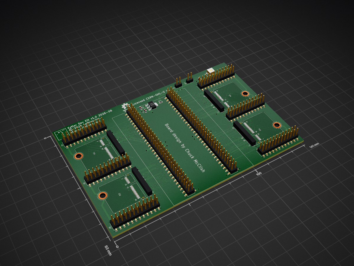
Devkyt is an open-source printed circuit board by Lattrex, from the Lattrex/devkyt repository on GitHub. It is a 4-layer board of 141 × 93 mm with 26 parts on 203 nets, routed with 6,325 tracks and 1,268 vias.
It is built around the LT3080IST#PBF, TSM-112-01-L-DV and CL21A106KAYNNNE, with the TSM-132-01-L-DV, RL0805FR-070R5L and 3314G-1-104E among its other parts. Its parts include 10 connectors, 3 capacitors, 1 resistor and 1 IC.


Open-source hardware carrier board for the Kyttar asynchronous DSP ASIC (SKY130 OpenFrame). The board hosts four Kyttar M.2 cards and plugs onto a ZTEX USB-FPGA Module 2.18b, giving a GNU Radio–driven development platform for the Kyttar array.
A passive carrier / breakout board:
It is receive-capable SDR / DSP development hardware, not a finished product.
Only the KiCad hardware design is published here right now. The FPGA gateware
and ZTEX SDK integration are coming later, once the bitstream-generation
flow is complete (they're intentionally excluded — see .gitignore).
devkyt/
├── LICENSE                         CERN-OHL-S v2 (hardware licence)
├── README.md                       this file
└── devkyt/                         the KiCad project
    ├── devkyt.kicad_pro            project
    ├── devkyt.kicad_sch            schematic
    ├── devkyt.kicad_pcb            4-layer PCB (fully routed, DRC-clean)
    ├── devkyt.kicad_dru            custom design rules (PCBWay 4-layer)
    ├── fab_overrides_pcbway.txt    fab floor for the autorouter (PCBWay 4L)
    ├── fp-lib-table / sym-lib-table  project-local library tables
    └── libraries/                  custom parts + reference docs
        ├── footprints/devkyt.pretty/   Kyttar M.2 socket, GND standoff, logo
        ├── symbols/devkyt.kicad_sym     custom symbols
        ├── PARTS.md                     parts inventory + provenance
        ├── OPENFRAME_GPIO_MAP.txt        Kyttar gpio ↔ M.2 pad map (verified)
        └── ZTEX_HEADER_MAP.txt           ZTEX 2.18b header pin map + mirror rule
Not yet in the repo (coming later):
fpga/ — FPGA gateware (the ZTEX↔Kyttar bridge / DDC).ztex/ — ZTEX SDK / firmware files.Fabricated as a 4-layer board (design rules target PCBWay; the
.kicad_dru and fab_overrides_pcbway.txt encode PCBWay's 4-layer capability).
devkyt.kicad_pcb
(File → Fabrication Outputs). Order 4-layer, 1oz, 1.6mm, HASL. Board is
~150 × 90 mm.| Ref | Part | MPN | Mfr |
|---|---|---|---|
| M1–M4 | M.2 E-key socket (MicroMod) | 2199230-4 | TE Connectivity |
| J1, J2 | 2×32 SMT vertical header | TSM-132-01-L-DV | Samtec |
| J4–J9 | 2×12 SMT vertical header | TSM-112-01-L-DV | Samtec |
| U1 | Adjustable LDO (Vcore) | LT3080 | Analog Devices |
Mates: ZTEX USB-FPGA Module 2.18b (bought separately).
devkyt/libraries/ — both were verified against the ChipFoundry Caravel M.2
card netlist, the SKY130 OpenFrame datasheet/RTL, and the ZTEX pinlist.ZTEX_HEADER_MAP.txt.Hardware is licensed under the CERN Open Hardware Licence Version 2 –
Strongly Reciprocal (see LICENSE). If you make or distribute
this hardware, or a modified version, you must make your design sources
available under the same licence and keep the source-location notice
(https://lattrex.com).
| Qty | Value | Footprint | References |
|---|---|---|---|
| 6 | Conn_02x12_Counter_Clockwise | Connector_PinHeader_2.54mm:PinHeader_2x12_P2.54mm_Vertical_SMD | J4, J5, J6, J7, J8, J9 |
| 4 | Kyttar 1 | devkyt:Kyttar_M.2-CONNECTOR-E | M1, M2, M3, M4 |
| 3 | , , | ||
| 2 | 10uF | Capacitor_SMD:C_0805_2012Metric | C1, C2 |
| 2 | ZTEX 2x32 | Connector_PinHeader_2.54mm:PinHeader_2x32_P2.54mm_Vertical_SMD | J1, J2 |
| 1 | 0.5 | Resistor_SMD:R_0805_2012Metric | R1 |
| 1 | 100k | Potentiometer_SMD:Potentiometer_Bourns_3314G_Vertical | RV1 |
| 1 | 1uF | Capacitor_SMD:C_0805_2012Metric | C3 |
| 1 | GND_Standoff | devkyt:Kyttar_GND_Standoff | H2 |
| 1 | ISHUNT | Connector_PinHeader_2.54mm:PinHeader_1x02_P2.54mm_Vertical | J3 |
| 1 | LOGO | devkyt:lattrex_logo | G*** |
| 1 | LT3080 | Package_TO_SOT_SMD:SOT-223-3_TabPin2 | U1 |
| 1 | OSHW-Logo_7.5x8mm_SilkScreen | Symbol:OSHW-Logo_7.5x8mm_SilkScreen | REF1 |
| 1 | VEXT | Connector_PinHeader_2.54mm:PinHeader_1x02_P2.54mm_Vertical | J10 |
It measures 141 × 93 mm and has 4 copper layers, 1.6 mm thick.
26 parts, built around the LT3080IST#PBF, TSM-112-01-L-DV, CL21A106KAYNNNE and TSM-132-01-L-DV. The full list of its parts is on this page, with links to each part's symbol and footprint where PCBKit's library has them.
From the Lattrex/devkyt repository on GitHub, at the commit this page was made from: the board is devkyt/devkyt.kicad_pcb and its schematic devkyt/devkyt.kicad_sch. PCBKit opens the board in the browser, with nothing to install.
Its repository states no licence, so its author keeps all rights: ask Lattrex before reusing the design.

jackw01/scanlight
A better light source for scanning color negative film

benkrasnow/1v2-boost-converter
Schematics and PCB layout for a boost converter 0.9V minimum input, 30A maximum input current


jrowe88/ecoport-bridge
CTA-2045 (EcoPort) bridge for a Rinnai REHP65 heat pump water heater


ste2425/PSP-Bluetooth
Formerly PSP-Consolizer, PSP-Bluetooth aims to add Bluetooth controller support to the PSP 1K/2K/3K.