2 layers57.1 × 48.5 mm
Power splitter
kylenmorris/reaction-chamber
A custom reaction chamber for automation of crop pathogens testing using a NAAT reaction, developed as a capstone project
30 parts

 kylenmorris/reaction-chamber
A custom reaction chamber for automation of crop pathogens testing using a NAAT reaction, developed as a capstone project
Main pcb is an open-source printed circuit board by kylenmorris, from the kylenmorris/reaction-chamber repository on GitHub. It is a 2-layer board of 163.5 × 133.5 mm with 56 parts on 81 nets, routed with 719 tracks and 99 vias.
It is built around the APDS-9006-020, LMC660CM and MCP3208-BI/P, with the B8B-XH-A, B6B-XH-AM and B02P-VL among its other parts. Its parts include 10 capacitors, 10 resistors, 3 connectors and 1 transistor.


Our capstone project was to design a self-contained device that would run Nucleic Acid Amplification Testing (NAAT), a method of in-field crop disease testing that replaces slow lab-based testing. This project was introduced to us by PathoScan who supplied the reaction tubes and supplies.
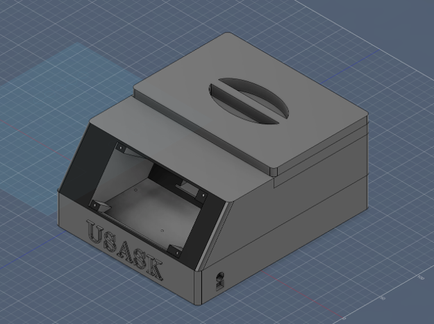
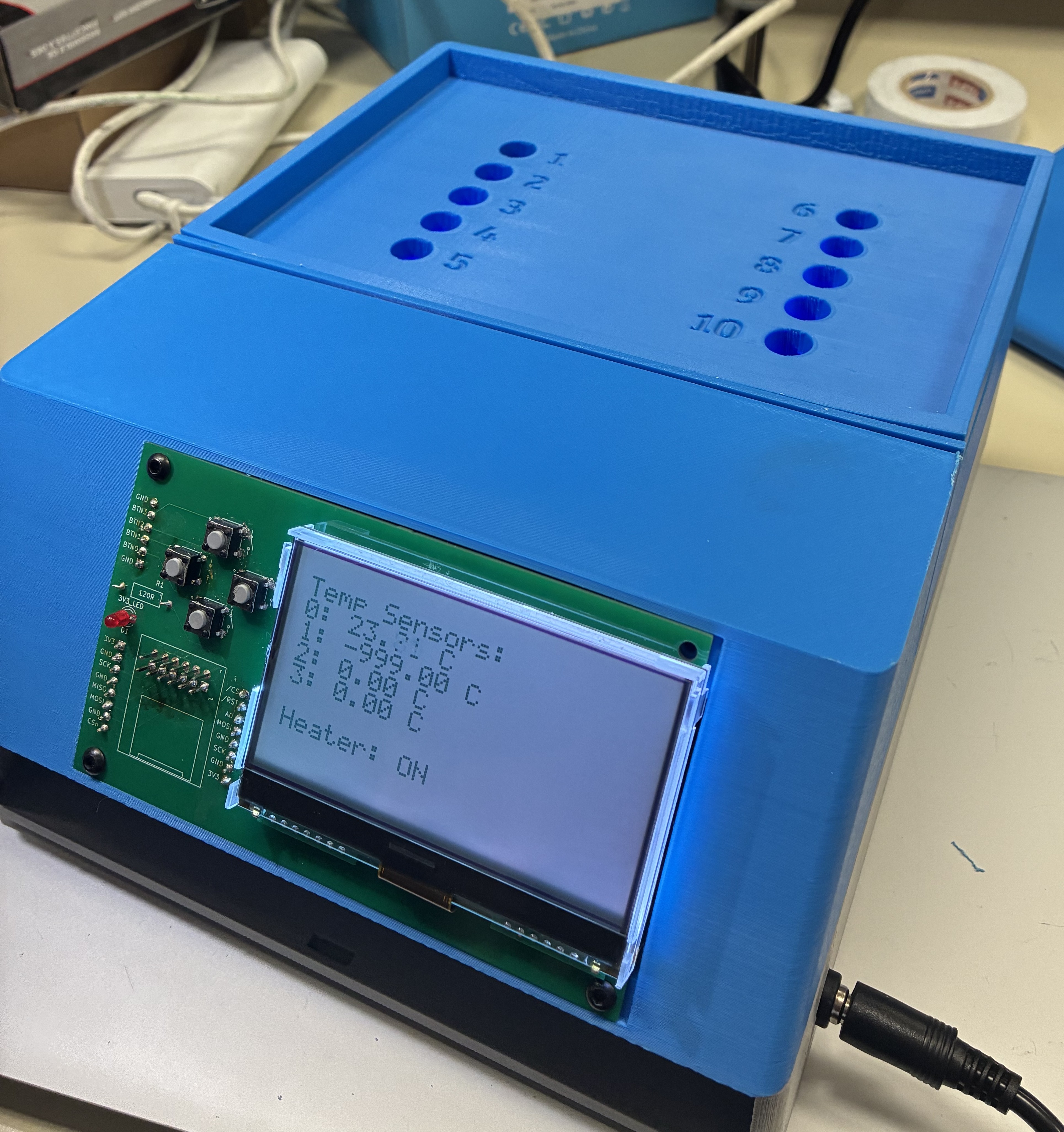
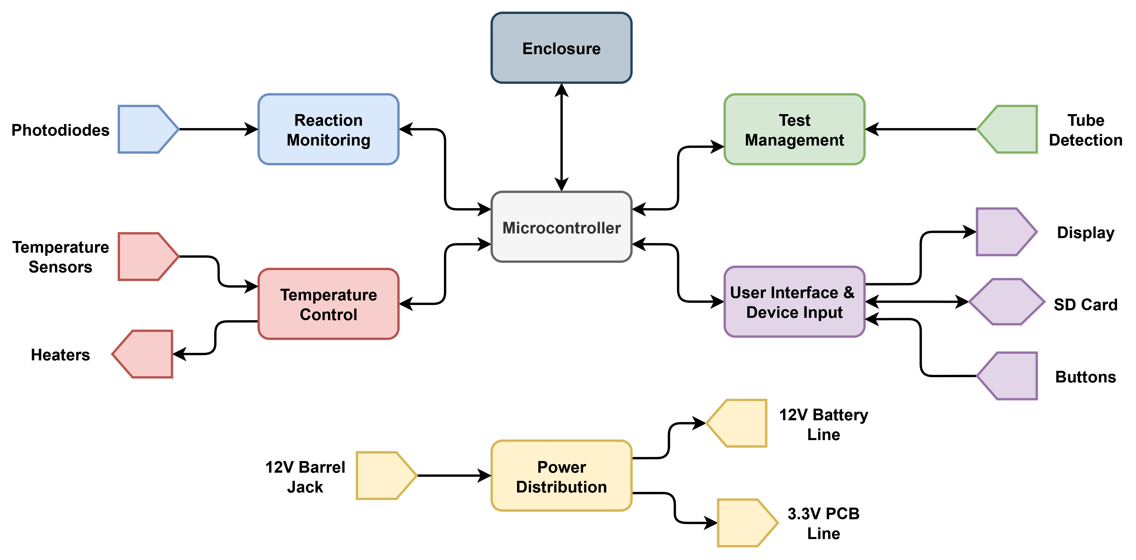
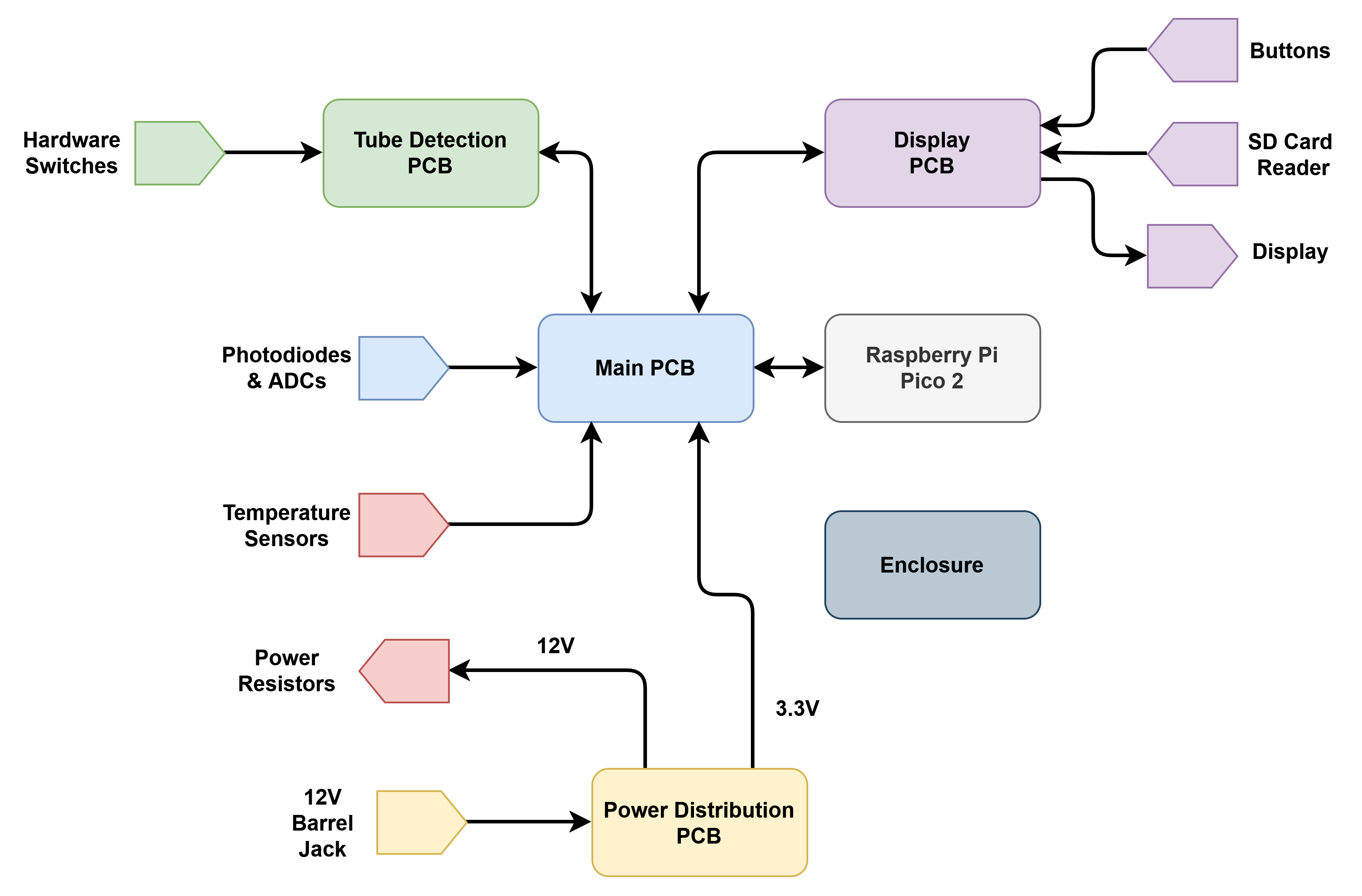
This device has several features, including maintaining and monitoring of internal chamber temperature, light-emission monitoring, storage of test results, and input/output from the user.
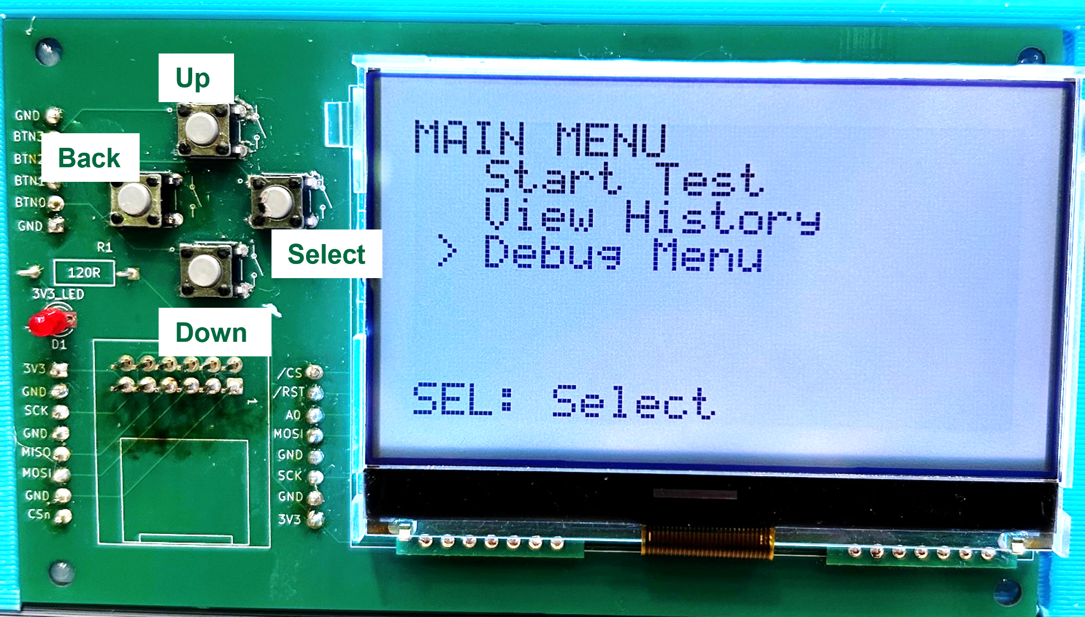
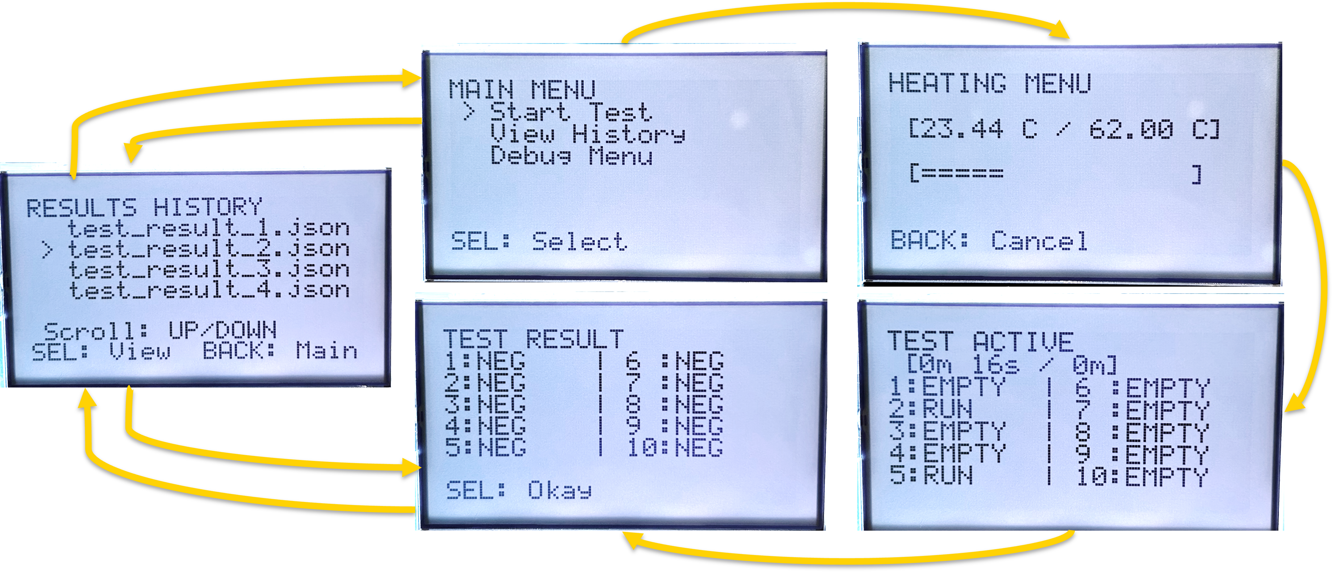
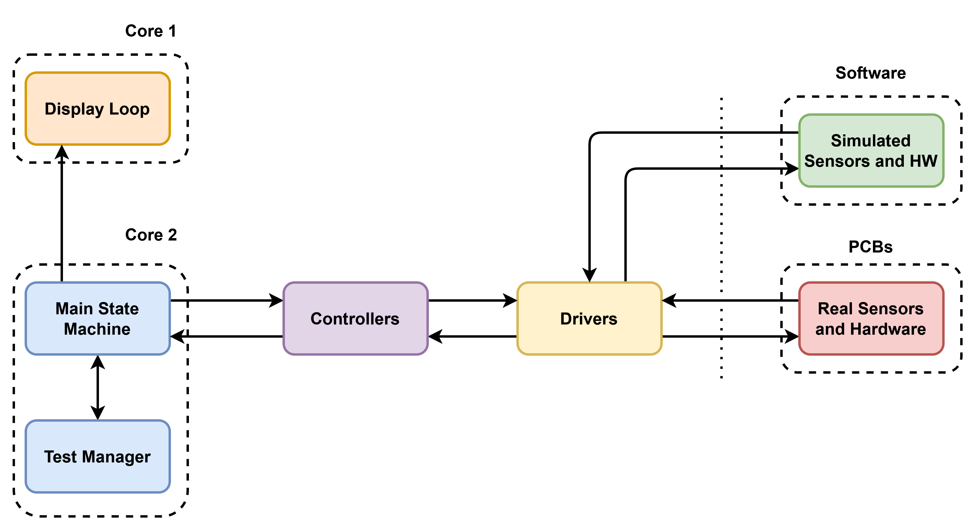
The system moves through seven states — BOOT, IDLE, HEATING, REACTING, RESULTS, HISTORY, and DEBUG.
We had successful heating to 50°C+ within 30 minutes, which was within spec. Our photodiodes and ADCs worked to capture the correct wavelength, and this was shown to the user and stored on the SD card, where it could be retrieved later.
The software allows for compile-time switching between the individual hardware components and a set of fake sensors. This allows us to run tests without all hardware being present, as well as running fully automated software tests.
Pull the project into your chosen directory
git clone https://github.com/kylenmorris/reaction-chamber.git Navigate into the /src directory
cd ./srcRun the docker compose file to build the .uf2 executable (found in ~/src/out/)
docker compose run firmwareFlash the Pico 2 by using the RPi VSCode extension or copying the file over manually (where E: is the Pico 2 on your system)
Copy-Item out\main.uf2 E:\ -ForceThe tests link the real logic_core against the simulated HAL, using run_system_state_loop_core0().
From the /src directory, configure a build and run it:
cmake -S . -B build_tests -DBUILD_TESTS=ON
cmake --build .\build_tests\
.\build_tests\Debug\test_main.exe
The test suite currently covers a few of the highest-value safety and operability checks:
TEMP_HIGH_HIGH_C, checked from every system stateHEATING-999C as seen in first pictureHEATING advances to REACTING once the chamber reaches targetSoftware
Hardware
Built for an industry partner - PathoScan - as part of a capstone project. The implementation is original work.
| Qty | Value | Footprint | References |
|---|---|---|---|
| 10 | 100p | Capacitor_SMD:C_1206_3216Metric_Pad1.33x1.80mm_HandSolder | C0, C1, C2, C3, C4, C5, C6, C7, C8, C9 |
| 10 | 8.25k | ul_MFP-25BRD52-10K:YAG_MF25_YAG | R0, R1, R2, R3, R4, R5, R6, R7, R8, R9 |
| 10 | APDS-9006-020 | APDS_9006_020:photodiode_v4 | Photo0, Photo1, Photo2, Photo3, Photo4, Photo5, Photo7, Photo8, Photo9, UPhoto6 |
| 6 | B8B-XH-A | Connector_JST:JST_XH_B8B-XH-A_1x08_P2.50mm_Vertical | LCD_Header1, SD_Header1, Temp0_Header1, Temp1_Header1, Temp2_Header1, Temp3_Header1 |
| 3 | B6B-XH-A | Connector_JST:JST_XH_B6B-XH-A_1x06_P2.50mm_Vertical | BTN_Header1, SW0_Header1, SW1_Header1 |
| 3 | LMC660CM | LMC660CMX_NOPB:SOIC127P600X175-14N | OpAmp1, OpAmp2, OpAmp3 |
| 2 | B02P-VL | B02P_VL:CONN_B02P-VL_JST | Power_Connector_3V3, Power_Connector_5V1 |
| 2 | B2B-XH-A | B2B_XH_A:JST_B2B-XH-A | Fan_Header1, Heater_Actuation1 |
| 2 | Conn_01x20_Socket | Connector_PinSocket_2.54mm:PinSocket_1x20_P2.54mm_Vertical | J1, J2 |
| 2 | MCP3208 | MCP3208_CI_P:DIP254P762X432-16 | ADC0, ADC1 |
| 1 | Conn_01x09_Socket | Connector_PinSocket_2.54mm:PinSocket_1x09_P2.54mm_Vertical | J3 |
| 1 | DMG2305UX-7 | DMG2305UX_7:SOT91P240X110-3N_DMG2305UX-7 | Q1 |
The 52 most common of 56 parts.
kylenmorris/reaction-chamber
A custom reaction chamber for automation of crop pathogens testing using a NAAT reaction, developed as a capstone project

kylenmorris/reaction-chamber
A custom reaction chamber for automation of crop pathogens testing using a NAAT reaction, developed as a capstone project

kylenmorris/reaction-chamber
A custom reaction chamber for automation of crop pathogens testing using a NAAT reaction, developed as a capstone project

RockSat-X/RSXVT2026
Our experiment aims to evaluate the use of optical navigation with Commercial-off-the-Shelf (COTS) products for use in spaceflight applications.

CNES/argos-demo-board
Demo board designed to use the ARRIBADA SMD module via USB to send ARGOS messages to the Kineis constellation.

themarcolab/Stardrive-Shield
With STARDRIVE SHIELD you can implement from 6 step to FOC motor control algorithms.


gustebeast/public-steel-guitar
A pedal steel guitar you can build yourself, from parts anyone can buy.


hwreverse/PokeConSound
Soundcard Designs for Pocket Computers (ポケコン) (Sharp, Casio, TRS80-M100,...)

yusufElnady/Medical-Imager
This repository contains the PCB design for a 16-channel ultrasound imager based on the K26 SOM and the TX7516 pulser.
It measures 163.5 × 133.5 mm and has 2 copper layers, 1.6 mm thick.
56 parts, built around the APDS-9006-020, LMC660CM, MCP3208-BI/P and B8B-XH-A. The full list of its parts is on this page, with links to each part's symbol and footprint where PCBKit's library has them.
From the kylenmorris/reaction-chamber repository on GitHub, at the commit this page was made from: the board is PCB/main_pcb/main_pcb/main_pcb.kicad_pcb and its schematic PCB/display-pcb/display-pcb.kicad_sch. PCBKit opens the board in the browser, with nothing to install.
Its repository states no licence, so its author keeps all rights: ask kylenmorris before reusing the design.