


4 layers30 × 16 mm
Layouts
kunichiko/MimicX-hardware
PCB designs (KiCad) for smart-retro-hid adapter boards
19 partsCERN-OHL-S-2.0

 kunichiko/MimicX-hardware
PCB designs (KiCad) for smart-retro-hid adapter boards
Layouts is an open-source printed circuit board by kunichiko, from the kunichiko/MimicX-hardware repository on GitHub, published under the CERN-OHL-S-2.0 licence. It is a 4-layer board of 50 × 40 mm with 34 parts on 61 nets, routed with 264 tracks and 46 vias.
Its parts include 10 resistors, 7 capacitors, 4 ICs, 4 diodes and 3 connectors. It belongs with the retro computing and games boards of this library.
製品名: Mimic X — 「Mimic X」プロジェクトのマイコン基板設計データ。
Mimic X is an open-hardware USB-MIDI adapter family that lets a phone (or any USB-MIDI / BLE-MIDI host) drive the real peripheral ports of 1980s Japanese computers — the Sharp X68000 keyboard/mouse port and the ATARI-standard 9-pin joystick port, including Mega Drive 6-button pads. This repository holds the board designs; the firmware, the protocol spec and the phone app live in the sibling repositories linked at the bottom.
LICENSE) — the .ato
sources, the KiCad layouts and the docs are all modifiable sources.
tools/ is Apache-2.0. Vendor-supplied symbols, footprints and 3D models
under <board>/parts/ are third-party and are not covered; see
NOTICE for the exact carve-out, the trademark terms and the
datasheet policy.0x1209:0x9210 (Mimic X) and 0x1209:0x9211 (Mimic X
Bridge), requested from pid.codes..kicad_sch and where to read the circuit instead.atari-joystick/ — ATARI / X68000 ジョイスティックアダプタD-SUB 9pin メス。X68000 / ATARI 標準ポートに直挿しし、メガドライブ 6 ボタン パッドもエミュレートする。rev 1.0.0、JLCPCB で製造済み。
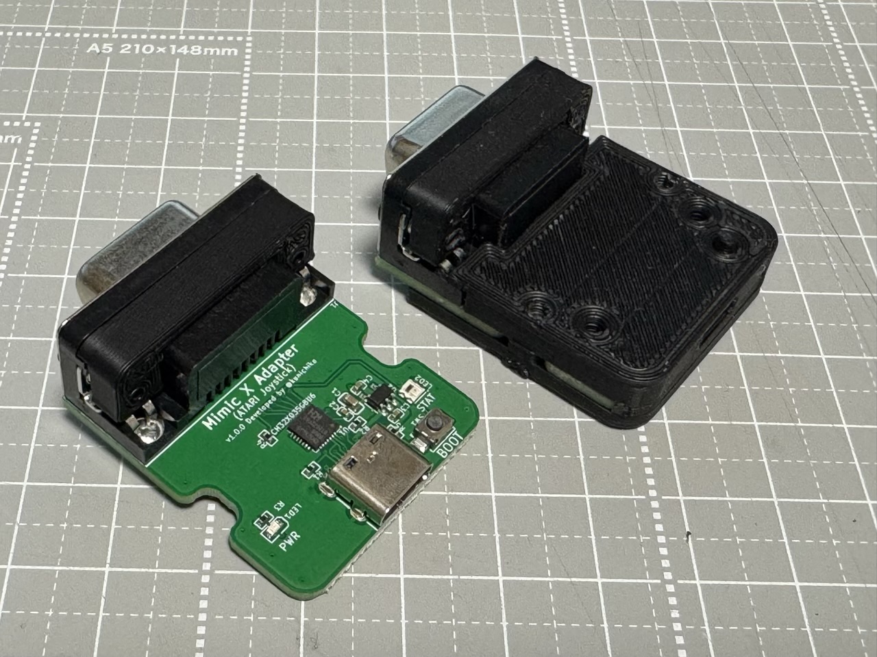
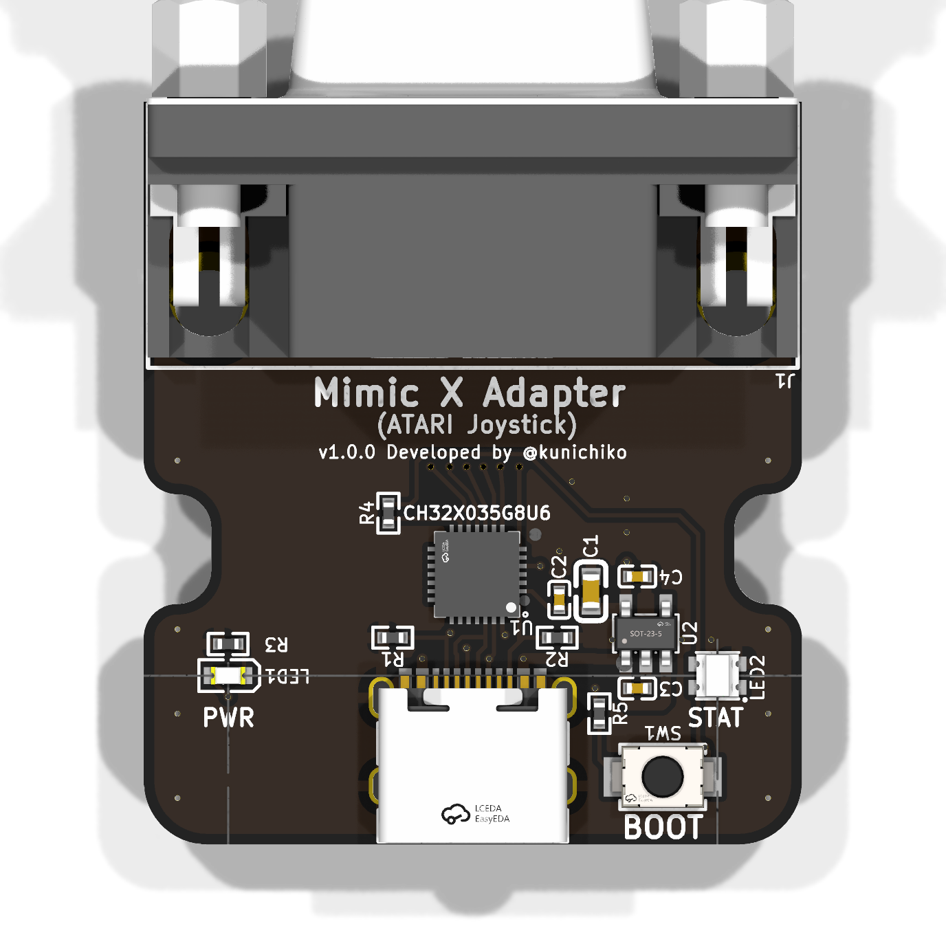
実装済みの基板と 3D プリントのケース (左) / KiCad レイアウトの 3D レンダ (右)。裏面と拡大は 基板 README を参照
| ブロック図 / block diagram | PDF · SVG |
| PCB レイヤープロット / layer plots | PDF (silk / Cu / fab, 6 pages) |
| 対話的に眺める / browse the layout | KiCanvas |
| 回路の定義 / circuit source | atari_joystick.ato |
| 製造データ / fabrication | layouts/default/production/ (Gerber + BOM + CPL) |
| 設計メモ / design notes | README.md |
x68000-keyboard/ — X68000 キーボード / マウスアダプタミニ DIN 7pin オス。X68000 のキーボード端子はマウス端子を兼用しており、本基板も 1 コネクタで両方をエミュレートする。4 層。rev 1.0.0、JLCPCB で製造済み。rev 1.0.1 (外形のセンターずれ修正) は未発注。
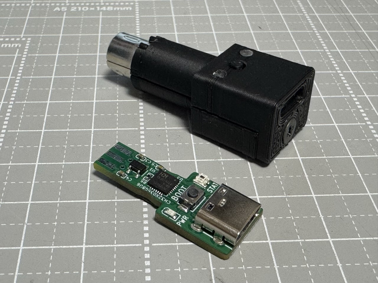
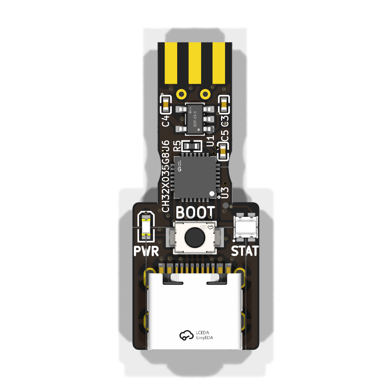
実装済みの基板と 3D プリントのケース (左) / KiCad レイアウトの 3D レンダ (右)。裏面と拡大は 基板 README を参照
| ブロック図 / block diagram | PDF · SVG |
| PCB レイヤープロット / layer plots | PDF (silk / Cu ×4 / fab, 8 pages) |
| 対話的に眺める / browse the layout | KiCanvas |
| 回路の定義 / circuit source | x68000_keyboard.ato |
| 製造データ / fabrication | layouts/default/production/ (Gerber + BOM + CPL) |
| 設計メモ / design notes | README.md |
wireless-combo/ — 無線 (BLE-MIDI) Combined アダプタXIAO ESP32-C6 (BLE-MIDI ホスト) + CH32X035 (デバイスエンジン) の 2 チップ構成で、 ジョイスティックとキーボードの両ポートを 1 枚で担当する。ESP32 が CH32 の電源と BOOT ピンを握っているため、CH32 のファームが壊れても SWD 経由で自力復旧できる。
rev 0.1 — 配線済み (4 層、DRC クリーン)、未発注。 3D レンダと レイヤープロットはまだ置いていない。回路の全体像はブロック図と
.atoを参照。
| ブロック図 / block diagram | PDF · SVG |
| 回路の定義 / circuit source | wireless_combo.ato |
| 設計メモ / design notes | README.md |
この 3 基板はいずれも atopile で設計している。atopile は
回路を「図」ではなく「コード」で書く EDA で、.ato から直接ネットリストと KiCad
レイアウトを生成する。したがって プロットできる回路図シート (.kicad_sch) は
そもそも存在しない。回路を読むには次のいずれかを使う:
These boards are designed in atopile, a text-based EDA: the circuit is written as code and the netlist and KiCad layout are generated from it. There is no schematic sheet to plot, so a reviewer has three ways in instead:
<board>/docs/*-block-diagram.pdf) — 全ブロック、全信号、
電源ドメイン、ピン割当表を 1 枚に収めた図。tools/gen_block_diagrams.py で
生成しており、内容は .ato の記述と 1:1 で対応する。
The closest thing to a schematic: every block, every net that leaves a
block, the power domains and the full pin map on one A4 sheet..ato ソース — 部品・接続・値・設計理由がコメント付きで書かれている
一次情報。~ が接続、~> が直列挿入を表す。
The primary source, with the reasoning in the comments.<board>/layouts/default/default.kicad_pcb) — 上の表の
KiCanvas リンクからブラウザで開ける。ネット名は .ato 側で
has_net_name により意味のある名前 (UP_3V3, KEY_TXD_3V3 など) に固定済み。
Browsable in KiCanvas; the nets carry meaningful names, not Net-(U1-Pad3).ブロック図とレイヤープロットの再生成:
# ブロック図 (SVG + PDF)。PDF は headless Chrome で出力する
python3 tools/gen_block_diagrams.py

# PCB レイヤープロット
KC=/Applications/KiCad/KiCad.app/Contents/MacOS/kicad-cli
$KC pcb export pdf --mode-multipage \
   --layers F.Silkscreen,F.Cu,B.Cu,B.Silkscreen,F.Fab,Cmts.User \
   --common-layers Edge.Cuts \
-o atari-joystick/docs/out atari-joystick/layouts/default/default.kicad_pcb| Qty | Value | Footprint | References |
|---|---|---|---|
| 5 | 100nF ±10% | Samsung_Electro_Mechanics_CL05B104KO5NNNC:C0402 | C3, C4, C5, C6, C7 |
| 4 | MountingHole_M3:MountingHole_M3 | H1, H2, H3, H4 | |
| 4 | 4.7kΩ ±1% | UNI_ROYAL_0402WGF4701TCE:R0402 | R2, R4, R9, R10 |
| 2 | TOSHIBA_TC7MPB9307FT_EL:TSSOP-20_L6.5-W4.4-P0.65-LS6.5-BL | U2, U3 | |
| 2 | B5819W_SOD123:B5819W_SOD123 | D1, D2 | |
| 2 | 100kΩ ±1% | UNI_ROYAL_0402WGF1003TCE:R0402 | R3, R5 |
| 2 | 10kΩ ±1% | UNI_ROYAL_0402WGF1002TCE:R0402 | R1, R6 |
| 1 | IDC_Header_2x04:IDC_Header_2x04 | J2 | |
| 1 | WCH_CH32X035G8U6:QFN-28_L4.0-W4.0-P0.40-BL-EP2.8 | U4 | |
| 1 | JST_XH_B3B:JST_XH_B3B | J3 | |
| 1 | AO3401A_SOT23:AO3401A_SOT23 | Q1 | |
| 1 | Worldsemi_WS2812B_2020_V6:LED-SMD_4P-L2.2-W2.0-P1.00_WS2815C-2020-4P | LED2 | |
| 1 | Hubei_KENTO_Elec_KT_0603G:LED0603-RD | LED1 | |
| 1 | XUNPU_TS_1088_AR02016:SW-SMD_L3.9-W3.0-P4.45 | SW1 | |
| 1 | IDC_Header_2x05:IDC_Header_2x05 | J1 | |
| 1 | XIAO_ESP32C6:XIAO_ESP32C6 | U1 | |
| 1 | 1kΩ ±1% | UNI_ROYAL_0402WGF1001TCE:R0402 | R7 |
| 1 | 22µF ±20% | Samsung_Electro_Mechanics_CL21A226MAQNNNE:C0805 | C1 |
| 1 | 4.7µF ±10% | Samsung_Electro_Mechanics_CL10A475KO8NNNC:C0603 | C2 |
| 1 | 470Ω ±1% | UNI_ROYAL_0402WGF4700TCE:R0402 | R8 |
kunichiko/MimicX-hardware
PCB designs (KiCad) for smart-retro-hid adapter boards

kunichiko/MimicX-hardware
PCB designs (KiCad) for smart-retro-hid adapter boards

kunichiko/MimicX-hardware
PCB designs (KiCad) for smart-retro-hid adapter boards

kunichiko/MimicX-hardware
PCB designs (KiCad) for smart-retro-hid adapter boards

kunichiko/MimicX-hardware
PCB designs (KiCad) for smart-retro-hid adapter boards


Ardumower/ardumower
Develop an open source robotic lawn mower (HW+SW reference platform)


lucanastasio/PCIexpress-KiCad
PCI express libraries and templates for KiCad


It measures 50 × 40 mm and has 4 copper layers, 1.6 mm thick.
34 parts. The full list of its parts is on this page, with links to each part's symbol and footprint where PCBKit's library has them.
From the kunichiko/MimicX-hardware repository on GitHub, at the commit this page was made from: the board is wireless-combo/layouts/default/default.kicad_pcb. PCBKit opens the board in the browser, with nothing to install.
Its repository publishes it under the CERN-OHL-S-2.0 licence: you may reuse it on that licence's terms (keep the author's notice, and for a copyleft licence share your changes alike).