4 layers100 × 272 mm
Mic array circuit
kevmck451/phase_array_fossn
develop a wide area coverage acoustic sensor with a 180 degree FOV and resolution sufficient to localize a target direction when combined with other sensing modalities
13 parts2
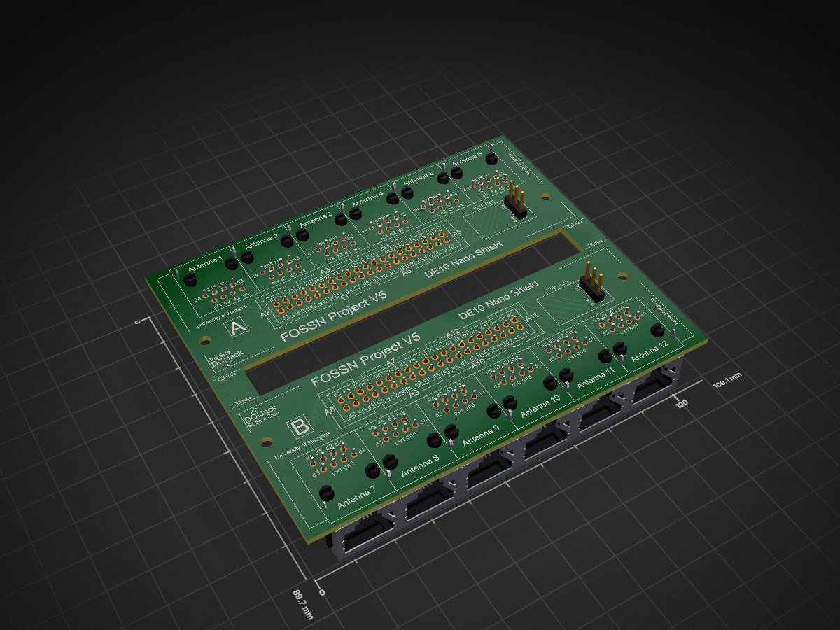
 kevmck451/phase_array_fossn2
develop a wide area coverage acoustic sensor with a 180 degree FOV and resolution sufficient to localize a target direction when combined with other sensing modalities
Antenna connector is an open-source printed circuit board by kevmck451, from the kevmck451/phase_array_fossn repository on GitHub. It is a 4-layer board of 109.1 × 89.7 mm with 20 parts on 9 nets, routed with 269 tracks and 0 vias.
It belongs with the radio and wireless and sensors and measurement boards of this library.
What they want from us: - easily deployable networked sensor system is needed to provide automated security monitoring - develop concepts for a Forward Operations Sensor Network
The sensor system should - detect encroaching personnel and vehicles (ground and aerial) - presence of chemical, biological, radiological, and nuclear (CBRN) materials - system of unattended sensors will communicate via a network - Autonomous algorithms will consolidate sensor inputs and provide summary notifications of activity within the area monitored to personnel in the FO unit
Results of this study: - a demonstration of several key technologies necessary for building an effective FOSSN - a detailed plan for the full development of the FOSSN
Complementary sensors of acoustic
Unattended Ground Sensors (UGS) Memphis has developed the means for implementing acoustic, magnetic, and hyperspectral sensors for UAS that can be translated to UGS sensing
The FOSSN team will translate these wide area coverage sensors into an UGS configuration and will demonstrate a VIS and LWIR capability for wide area coverage to include the detection and recognition of humans and vehicles. The FOSSN team will also perform field experimentation to determine the performance of these systems in the range at which these systems effectively engage humans and military vehicles, including threat UAS.
The FOSSN team will also leverage existing phased array acoustic sensing to a UGS configuration
All sensors will be tied together leveraging Named Data Networking (NDN) and multi-hop ad hoc communications developed for the ARL program
Based on prior experience and input from task 3.1, research areas needed for the development of a complete and operationally effective system will be developed. For each area, recommendations regarding technical approaches will be made and a report produced.
3.4.2 Phased Array Acoustic Sensor Research - The FOSSN team will develop a wide area coverage acoustic with at least a 180 degree FOV with resolution sufficient to localize a target direction when combined with other sensing modalities. This sensor will leverage technologies developed for the UAS based acoustic interrogator mission. - The FOSSN team will demonstrate the acoustic UGS systems in the field. The system will be demonstrated in the field with a ground sensor coupled to a tabletop computer that can show the performance of the system. - The FOSSN team will determine the performance of the wide area acoustic system. A theoretical performance will be provided as well as a field experiment/demonstration that provides the range at which aerial and ground vehicles can be detected and recognized.
The FOSSN team will develop an overall plan for developing a system that meets the needs of field artillery security. This plan will detail any needed technology development and the necessary resources to execute the plan.
Test and Evaluation (T&E) Plan – Based on the results of laboratory and field evaluations and demonstrations, an overall T&E plan will be developed for a complete field artillery security system.
kevmck451/phase_array_fossn
develop a wide area coverage acoustic sensor with a 180 degree FOV and resolution sufficient to localize a target direction when combined with other sensing modalities

hackclub/OnBoard
💡 Join 1,000 teenagers and make your first PCB with a $100 grant!

JanM321/esphome-lg-controller
Wired controller for LG HVAC units using ESPHome and ESP32


RespiraWorks/Ventilator
Fully-featured ICU ventilator design, optimized for manufacture using commonly available components and free to license.

dbalsom/arduinoX86
An interface between an Arduino Due or Arduino GIGA and 8088, 8086, V20, V30, 186 or 286 CPUs

lukasloetkolben/OpenpilotHardware
Welcome to the Openpilot Hardware Collection!

macaba/TheManhattanToolkit
Input R - RNCF0603DTE10R0 (10 ohm) Input CM C - CGA3E1C0G2A472J080AC (4.7nF) Input DM C - DNP

It measures 109.1 × 89.7 mm and has 4 copper layers, 1.6 mm thick.
20 parts. The full list of its parts is on this page, with links to each part's symbol and footprint where PCBKit's library has them.
From the kevmck451/phase_array_fossn repository on GitHub, at the commit this page was made from: the board is Circuit_Boards/DE10_Shield/DE10_Shield_KiCad/antenna_connector.kicad_pcb and its schematic Circuit_Boards/DE10_Shield/DE10_Shield_KiCad/antenna_connector.kicad_sch. PCBKit opens the board in the browser, with nothing to install.
Its repository states no licence, so its author keeps all rights: ask kevmck451 before reusing the design.