6 layers75 × 135.2 mm
Dumpling Main
nyuad-space/dumpling
Modular payload for high-speed logging and benchmarking of COTS sensors, enabling real-world performance data and open sharing.
370 parts1

 kabidey/someda-claude-plugin
This plugin puts the someda engine behind three slash commands. In a conversation, Claude writes the circuit as a small JSON plan: real parts with datasheet pinouts, nets, and intent such as "USB-C on the top edge".
Evidence is an open-source printed circuit board by kabidey, from the kabidey/someda-claude-plugin repository on GitHub, published under the MIT licence. It is a 6-layer board of 90 × 60 mm with 132 parts on 114 nets, routed with 1,708 tracks and 470 vias.
It is built around the W25Q128JVSIQ, TPS562200DDC and ME6211C18M5G-N, with the USBLC6-2SC6, XC6206P302MR and M2.5 among its other parts. Its parts include 59 capacitors, 43 resistors, 8 connectors, 7 ICs and 3 inductors.


Describe a circuit; get a fab-ready KiCad project with every claim checked.
This plugin puts the someda engine behind three slash commands. In a conversation, Claude writes the circuit as a small JSON plan: real parts with datasheet pinouts, nets, and intent such as "USB-C on the top edge". Never a coordinate. The compiled engine does the rest: schematic, footprints, placement, routing (differential pairs, enforced crosstalk spacing), signal-integrity / stability / thermal audits, KiCad's own ERC and DRC, Gerbers, drill, BOM, a JLCPCB order package and 3D renders. The build ends with six gates; all six pass or the answer is NOT DONE with the failing gate named.
The engine repairs what a plan edit can fix (a misspelled footprint, a missing decoupling capacitor, a regulator short of output capacitance, a connector with no room on its edge) and builds again, so the plan can come from a small model, a large one, or a person.
claude plugin marketplace add kabidey/someda-claude-plugin
claude plugin install someda@someda
On first use the plugin resolves the engine: someda on your PATH, a SOMEDA_BIN override, or
the release binary for your platform (Linux x86_64, macOS Apple silicon and Intel, Windows
x86_64; other platforms are built from source with cargo). It also installs what a build
needs beyond the binary: KiCad's footprint and 3D model libraries (apt on Debian/Ubuntu) and
the LCSC/EasyEDA converter in a private virtualenv.
You need KiCad with kicad-cli on your PATH (developed and verified
against KiCad 10.0.6). No API key is required: Claude is the planner.
Not using Claude Code? The same release archive the plugin downloads also holds someda-app,
a desktop window that does the whole flow with any language model provider (see the
engine README).
you:     /pcb-plan a 555 timer blinking an LED at about 1 Hz, 5 V in on a header
claude:  writes plan.json (NE555, timing RC, LED and resistor, 100 nF next to the 555,
         a 2-pin header on the left edge) and shows it for review

you:     /pcb-build 555 LED blinker
claude:  1. schematic written and exported to PDF for your approval
         2. fetch-libs: every footprint and 3D model FOUND or FETCHED (none MISSING)
         3. the engine builds: placement ✓  routed 15 of 15 ✓  audits ✓
            kicad-cli ERC ✓ DRC 0 errors ✓  Gerbers / drill / BOM / JLCPCB package / renders ✓
            export preflight: drc shorts unrouted pours gerbers drill = 6 / 6
         → someda-build/circuit.kicad_pcb, fab/, fab/jlcpcb/, render/, plan.built.json
Those numbers are the engine's quick-start plan (examples/plan_555.json) built with someda 0.7.0 and kicad-cli 10.0.6.
| Command | What it does |
|---|---|
/pcb-plan <description> | Write plan.json following the contract and show it. No build. |
/pcb-build <description> | Schematic for approval → libraries fetched → build with the engine's repair rounds → honest report of every stage and gate. |
/pcb-check <file> | The engine's DRC/ERC on an existing .kicad_pcb or .kicad_sch. |
The build step in detail:
scripts/fetch-libs.py pulls every footprint and 3D model the plan needs that your KiCad libraries lack: KiCad's GitLab repositories, LCSC/EasyEDA by lcsc part number (or mpn, resolved through JLCPCB's parts search), and KiCad zips you downloaded from UltraLibrarian, SnapEDA, Mouser or Digi-Key (--import). Every part ends FOUND, FETCHED (with its source) or MISSING with the plan edit to make. A MISSING name that is only a misspelling is corrected by the engine's first repair round; a part the libraries really lack is never guessed.someda ai build runs up to SOMEDA_REPAIR_ROUNDS (default 3) repair rounds by itself, printing repair: for what it changed and suggest: with the exact plan edit for what it could not; the plan as built is someda-build/plan.built.json.Placement from real courtyards (mounting holes at their corners, edge connectors rotated so their opening faces the edge and placed on it, parts next to the pins they share, keep-out rings for fine-pitch escapes); routing on JLCPCB rules for 2, 4 or 6 layers with inner planes and per-pad fanouts, escape vias for fine-pitch pins, differential pairs as coupled corridors with matched lengths, 3W/5W crosstalk spacing enforced for every fast net; audits on the routed copper (stray L/C, SWR, unterminated lines, crosstalk re-measured, decoupling loop inductance, regulator and crystal checks, PDN |Z(f)|, junction temperatures, JLCPCB scope); kicad-cli ERC and DRC judged from the report file; Gerbers, drill, position, detailed BOM, JLCPCB order package (Protel-named zip, assembly BOM, CPL with rotation corrections), 3D renders with component bodies. The engine README has the full list and the plan fields.
examples/sompi-v3s is an Allwinner V3s single-board computer planned this way: 132 parts on 90 × 60 mm, six layers, USB-C, 10/100 Ethernet, microSD, SPI NOR, 40-pin LCD and 24-pin MIPI camera FPCs, audio jack, GPIO header, two bucks and two LDOs. With someda 0.7.0 it routes 187 of 187 connections, couples all seven USB / Ethernet / MIPI pairs within their skew budgets, has 0 crosstalk violations and kicad-cli DRC 0 errors, and passes the six gates. The engine rotated every edge connector from its footprint, moved the audio jack to the bottom edge when the top edge had no slot deep enough, and grew the 1.8 V plane island to reach its capacitors. Its remaining warnings are real and listed (crystal traces of 11–17 mm, one far capacitor, three capacitors beyond the island, board density 147 %).
The unedited outputs of that build (Gerbers, KiCad project, DRC and ERC reports, schematic PDF, renders, BOM, JLCPCB package, checksums) are in examples/sompi-v3s/evidence.
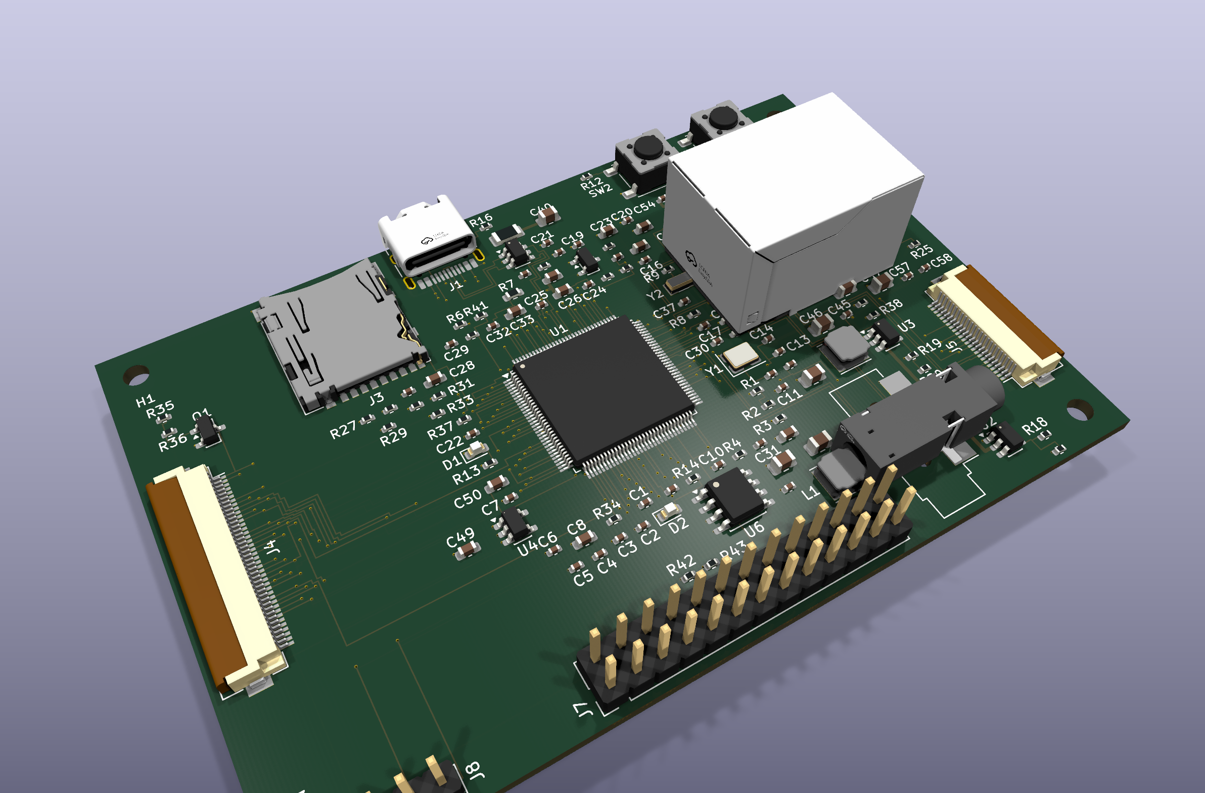
The boards are not simulated and have not been built. Connector pinouts follow conventions that must be checked against the parts you buy; 3D bodies fetched from LCSC are not verified against physical parts; clock-to-data skew across pairs is not enforced; everything is placed on the top side. Read the warnings; they are the engine telling you what it could not make good.
commands/            pcb-plan, pcb-build, pcb-check
skills/someda/       SKILL.md: how Claude plans and runs a build; references/CONTRACT.md: the plan
scripts/             setup-someda.sh (engine + libraries), fetch-libs.py (footprints and 3D models)
examples/sompi-v3s/  the SBC plan, its generator, design notes and build evidence
MIT license · SomTronics
| Qty | Value | Footprint | References |
|---|---|---|---|
| 34 | 100nF | Capacitor_SMD:C_0402_1005Metric | C1, C2, C10, C11, C12, C13, C14, C16, C17, C18, C19, C20, C21, C22, C24, C25 +18 |
| 8 | 10uF | Capacitor_SMD:C_0603_1608Metric | C8, C15, C23, C26, C27, C28, C33, C50 |
| 7 | 10k | Resistor_SMD:R_0402_1005Metric | R27, R28, R29, R30, R31, R33, R36 |
| 4 | 22uF | Capacitor_SMD:C_0805_2012Metric | C43, C44, C47, C48 |
| 4 | 2k 1% | Resistor_SMD:R_0402_1005Metric | R1, R2, R3, R4 |
| 4 | 4.7k | Resistor_SMD:R_0402_1005Metric | R38, R39, R42, R43 |
| 4 | 51R 1% | Resistor_SMD:R_0402_1005Metric | R21, R22, R23, R24 |
| 4 | M2.5 | MountingHole:MountingHole_2.7mm_M2.5 | H1, H2, H3, H4 |
| 3 | 10uF | Capacitor_SMD:C_0805_2012Metric | C40, C42, C46 |
| 3 | 1k | Resistor_SMD:R_0402_1005Metric | R13, R14, R35 |
| 3 | 1uF | Capacitor_SMD:C_0603_1608Metric | C49, C51, C52 |
| 3 | 33R | Resistor_SMD:R_0402_1005Metric | R32, R34, R37 |
| 2 | 10k 1% | Resistor_SMD:R_0402_1005Metric | R18, R20 |
| 2 | 18pF | Capacitor_SMD:C_0402_1005Metric | C34, C35 |
| 2 | 1uF | Capacitor_SMD:C_0402_1005Metric | C32, C38 |
| 2 | 330R | Resistor_SMD:R_0402_1005Metric | R25, R26 |
| 2 | 4.7uH 3A | Inductor_SMD:L_Taiyo-Yuden_NR-40xx | L1, L2 |
| 2 | 5.1k | Resistor_SMD:R_0402_1005Metric | R15, R16 |
| 2 | 6pF | Capacitor_SMD:C_0402_1005Metric | C36, C37 |
| 2 | TPS562200 | Package_TO_SOT_SMD:SOT-23-6 | U2, U3 |
| 1 | 0R | Resistor_SMD:R_0402_1005Metric | R41 |
| 1 | 0R | Resistor_SMD:R_0603_1608Metric | R7 |
| 1 | 100k 1% | Resistor_SMD:R_0402_1005Metric | R11 |
| 1 | 10M | Resistor_SMD:R_0402_1005Metric | R9 |
| 1 | 10uH | Inductor_SMD:L_0805_2012Metric | L3 |
| 1 | 1nF | Capacitor_SMD:C_0402_1005Metric | C39 |
| 1 | 200k 1% | Resistor_SMD:R_0402_1005Metric | R6 |
| 1 | 22R | Resistor_SMD:R_0402_1005Metric | R40 |
| 1 | 240R 1% | Resistor_SMD:R_0402_1005Metric | R5 |
| 1 | 24MHz | Crystal:Crystal_SMD_3225-4Pin_3.2x2.5mm | Y1 |
| 1 | 2A fuse | Fuse:Fuse_1206_3216Metric | F1 |
| 1 | 3.5mm jack | Connector_Audio:Jack_3.5mm_CUI_SJ-3523-SMT_Horizontal | J6 |
| 1 | 32.768kHz | Crystal:Crystal_SMD_3215-2Pin_3.2x1.5mm | Y2 |
| 1 | 33.2k 1% | Resistor_SMD:R_0402_1005Metric | R17 |
| 1 | 47k | Resistor_SMD:R_0402_1005Metric | R10 |
| 1 | 5.62k 1% | Resistor_SMD:R_0402_1005Metric | R19 |
| 1 | 6.04k 1% | Resistor_SMD:R_0402_1005Metric | R8 |
| 1 | 6.8k 1% | Resistor_SMD:R_0402_1005Metric | R12 |
| 1 | AO3400A | Package_TO_SOT_SMD:SOT-23 | Q1 |
| 1 | Allwinner V3s | SomPi:eLQFP-128_14x14mm_P0.4mm_EP5.72x5.72mm_ThermalVias | U1 |
| 1 | CAM MIPI 24P | Connector_FFC-FPC:Hirose_FH12-24S-0.5SH_1x24-1MP_P0.50mm_Horizontal | J5 |
| 1 | GPIO 2x13 | Connector_PinHeader_2.54mm:PinHeader_2x13_P2.54mm_Vertical | J7 |
| 1 | KEY1 | Button_Switch_SMD:SW_SPST_PTS645Sx43SMTR92 | SW2 |
| 1 | LCD 40P RGB | Connector_FFC-FPC:Hirose_FH12-40S-0.5SH_1x40-1MP_P0.50mm_Horizontal | J4 |
| 1 | ME6211C18M5G | Package_TO_SOT_SMD:SOT-23-5 | U4 |
| 1 | PWR red | LED_SMD:LED_0603_1608Metric | D1 |
| 1 | RESET | Button_Switch_SMD:SW_SPST_PTS645Sx43SMTR92 | SW1 |
| 1 | RJ45 HR911105A | Connector_RJ:RJ45_Hanrun_HR911105A_Horizontal | J2 |
| 1 | STAT green | LED_SMD:LED_0603_1608Metric | D2 |
| 1 | UART0 debug | Connector_PinHeader_2.54mm:PinHeader_1x03_P2.54mm_Vertical | J8 |
| 1 | USB-C 16P | Connector_USB:USB_C_Receptacle_HRO_TYPE-C-31-M-12 | J1 |
| 1 | USBLC6-2SC6 | Package_TO_SOT_SMD:SOT-23-6 | U8 |
| 1 | W25Q128JVSIQ | Package_SO:SOIC-8_3.9x4.9mm_P1.27mm | U6 |
| 1 | XC6206P302MR | Package_TO_SOT_SMD:SOT-23 | U5 |
| 1 | microSD | Connector_Card:microSD_HC_Hirose_DM3AT-SF-PEJM5 | J3 |
nyuad-space/dumpling
Modular payload for high-speed logging and benchmarking of COTS sensors, enabling real-world performance data and open sharing.


Ben-Blair/Rocket-Build
Senior capstone project: demonstrate closed-loop lateral guidance of a high power rocket using forward canards, and handle the canard-wake-on-aft-fin interference problem correctly.

Brillar0101/agentdeck
RP2040 macropad for supervising AI coding agents: 13 hot-swap keys with per-key RGB status, encoder, joystick, 4-layer PCB, CircuitPython firmware, printable enclosure

jmcpheron/pico-quorum
Several people, several keys, one Safe. Hardware approvals for Safe multisig wallets.

Andreuxxx1977/esp32-p4
An open-hardware, actively cooled ESP32-P4 board for heavy multimedia work: a 2-lane MIPI camera, a 2-lane MIPI display, USB 2.0 High-Speed, 10/100 Ethernet, UHS-I microSD, 32 MB flash and 32 MB PSRAM.

SebastianKristo/pult-forsterker
Ett kort (180 × 100 mm, 2 lag) som erstatter alle modulene, og som i tillegg har USB-delingsswitch, to AUX-innganger som digitaliseres (så alt kan mikses), «smart relé» for strømmen til forsterkerdelen…

rmingon/ScrapHawk
An ultra-budget, high-performance drone flight controller powered by the RP2040. Featuring a full 9-axis navigation stack, GPS, dual-stage power filtering, and a dual-core FreeRTOS architecture.
It measures 90 × 60 mm and has 6 copper layers, 1.6 mm thick.
132 parts, built around the W25Q128JVSIQ, TPS562200DDC, ME6211C18M5G-N and USBLC6-2SC6. The full list of its parts is on this page, with links to each part's symbol and footprint where PCBKit's library has them.
From the kabidey/someda-claude-plugin repository on GitHub, at the commit this page was made from: the board is examples/sompi-v3s/evidence/kicad/circuit.kicad_pcb and its schematic examples/sompi-v3s/evidence/kicad/circuit.kicad_sch. PCBKit opens the board in the browser, with nothing to install.
Its repository publishes it under the MIT licence: you may reuse it on that licence's terms (keep the author's notice, and for a copyleft licence share your changes alike).