2 layers41 × 19 mm
TiniFlex
INTI-CMNB/Curso-KiCad-Intro
Curso introductorio al uso de KiCad, con modalidad taller, armado a solicitud del proyecto CIAA
13 parts3

 joshbressers/badge10
An open source badge
Badge is an open-source printed circuit board by joshbressers, from the joshbressers/badge repository on GitHub, published under the Apache-2.0 licence. It is a 2-layer board of 76.2 × 113 mm with 99 parts on 56 nets, routed with 635 tracks and 87 vias.
It is built around the ATTINY85-20SF, SN74HC595D and CD4021BE, with the TL3315NF160Q and BS-7 among its other parts. Its parts include 64 diodes, 16 resistors, 6 switches and 4 ICs. It belongs with the lEDs and displays boards and the AVR (ATmega, ATtiny) boards of this library.


This code is no longer maintained, everything got too complicated. You should go to the new home of this project https://github.com/OpenBadgeProject
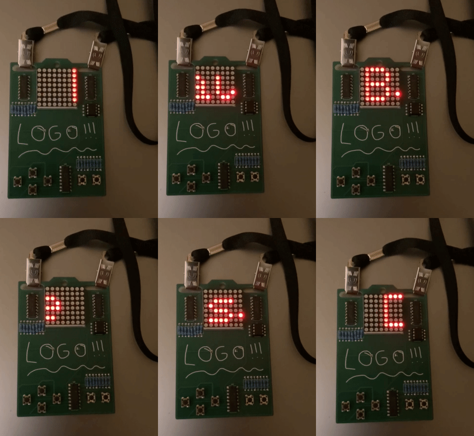
This is the Open Badge Project. The idea behind this is to have a very low cost, low power electronic badge. These could be built just for fun, or if you're throwing a conference, feel free to use the PCB as the badge, maybe build some, maybe let the folks at the conference build them.
Electronic badges have gotten pretty hip, but they seem to suffer from two primary problems.
The goal of the Open Badge Project was to build a badge that costs $5 or less and can run for a day or more on one 2032 battery.
The badge as it stands right now will only cost $5 if you build A LOT (1000 or more). The cost is closer to $6 or $7 for smaller batches at the moment, but that's still pretty reasonable.
There are two versions of the badge. One is a through hole badge that's very easy to solder. It was designed with human fabricators in mind. The kicad files in the main branch are for the through hole model.
There is also a surface mount version in the surface-mount branch. This version of the badge can be sent off to a fabricator to be mass produced.
Both badge versions use the same code.
The badge itself runs on a microprocessor called an ATTINY85. It has 8K of program space, 512 bytes (yes, bytes) of memory. That microprocessor then drives 3 shift registers. One for the button input, and two for the display output. Shift registers shouldn't be used to drive LEDs, but it works, and doing it this way keeps the cost down.
The PCB can be shipped off to one of the countless PCB manufacturers that exist. There is room on the front for a logo. There is also plenty of room on the back for graphics. Instructions for swapping in your own logo can be found below.
The PCB was designed using KiCad, version 7.0 to be precise. Your mileage may very if you try to use other versions.
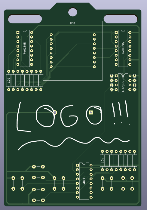
You can generate a bill of materials from KiCad, but for the sake of simplicity here is a list of all the parts.
There may be better places to purchase these things than these links. Please submit a PR if you find something better.
KiCad has a tool called "Image Converter". This application lets you turn an image into a footprint that can be added to the PCB layout.
When you run the tool, there is a button on the left called "Load Source Image". If you have a black and white image to start with that's the best. You can use any image but things get weird.
Once you load an image you will need to watch the size. The "Output Size" field is what matters here. It will take a few tries to get it right. There's about 3 inches by 1.7 inches of space to work with on the front.
Use the "Front Solder Mask" layer. Make sure you use Footprint for the output layer.
Click Export to file. Save the file in the badge-footprints.pretty directory.
Now open the "PCB Editor" application. Make sure the "F. Silkscreen" layer is selected on the right.
You will have to click on and delete the existing logo. Now from the menu Place -> Add Footprint
If you search for "badge" in the text box you should see your logo show up in the list. Double click it, then place it where it fits. If the logo isn't sized right, go back to the Image Converter and try again.
If you want to have PCBs made, you need to export the Gerber files from the PCB Editor. The Gerber files are what you send the PCB manufacturer.
Run the PCB Editor, then File -> Fabrication Outputs -> Gerbers
Create a new directory to hold the files (there will be more than one). For example let's call it badge_gerber. Leave the default settings alone, it should do the right thing.
Then click Plot. Then click "Generate Drill Files" and "Generate Drill File" on the window that pops up. Your directory now has the files need to create the PCB in it.
The PCB manufacturer will want that directory turned into a zip file and uploaded. You're on your own to figure that part out.
In order to program the ATTINY85 you will need a programmer. There is a lovely page that explains how to use an arduino as your programmer
The reset pin on this chip is special. We are purposely not using that pin (so we really only have 5 IO pins now) because if you use the reset pin, you now require a high voltage programmer. Since we want people to program this thing using only an arduino, we'll keep the reset pin free.
See DEVELOPING.md
| Qty | Value | Footprint | References |
|---|---|---|---|
| 64 | LED | LED_SMD:LED_1206_3216Metric_Pad1.42x1.75mm_HandSolder | D1, D2, D10, D11, D12, D13, D14, D15, D16, D17, D18, D19, D20, D21, D22, D23 +48 |
| 8 | 100 | PCM_JLCPCB:R_0805 | R1, R2, R3, R4, R5, R6, R7, R8 |
| 8 | 10k | PCM_JLCPCB:R_0805 | R9, R10, R11, R12, R13, R14, R15, R16 |
| 8 | TestPoint | TestPoint:TestPoint_THTPad_D1.5mm_Drill0.7mm | TP1, TP2, TP3, TP4, TP5, TP6, TP7, TP8 |
| 5 | C83206 | Badge-Library:C83206 | S2, S3, S4, S5, S6 |
| 2 | SN74HC595 | PCM_JLCPCB:SOIC-16_L9.9-W3.9-P1.27-LS6.0-BL | U3, U4 |
| 1 | ATtiny85-20SF | Package_SO:SOIC-8_5.3x5.3mm_P1.27mm | U1 |
| 1 | C83206 | Button_Switch_SMD:SW_MEC_5GSH9 | S1 |
| 1 | CD4021B | PCM_JLCPCB:SOIC-16_L9.9-W3.9-P1.27-LS6.0-BL | U2 |
| 1 | CR2032 | Battery:BatteryHolder_MPD_BC2003_1x2032 | BAT1 |
INTI-CMNB/Curso-KiCad-Intro
Curso introductorio al uso de KiCad, con modalidad taller, armado a solicitud del proyecto CIAA


CCHS-Melbourne/vend-matrix
This is the CCHS Vending Machine motor controller.

Sirotaca/SNES-Arcade-Controller-PCB
PCB for DIY arcade-style controllers for SNES


Alberta2514640/EIT-Machine
Arbitrary Waveform Generator for the Raspberry Pi Pico 16 Channels
It measures 76.2 × 113 mm and has 2 copper layers, 1.6 mm thick.
99 parts, built around the ATTINY85-20SF, SN74HC595D, CD4021BE and TL3315NF160Q. The full list of its parts is on this page, with links to each part's symbol and footprint where PCBKit's library has them.
From the joshbressers/badge repository on GitHub, at the commit this page was made from: the board is kicad/badge.kicad_pcb and its schematic kicad/badge.kicad_sch. PCBKit opens the board in the browser, with nothing to install.
Its repository publishes it under the Apache-2.0 licence: you may reuse it on that licence's terms (keep the author's notice, and for a copyleft licence share your changes alike).