
2 layers100 × 80 mm
Robot main
johnugbor/RoboSolar
SKiDL-generated draft v0.1. NOT FOR FABRICATION — see blockers below.
78 partsMIT
 johnugbor/RoboSolar
SKiDL-generated draft v0.1. NOT FOR FABRICATION — see blockers below.
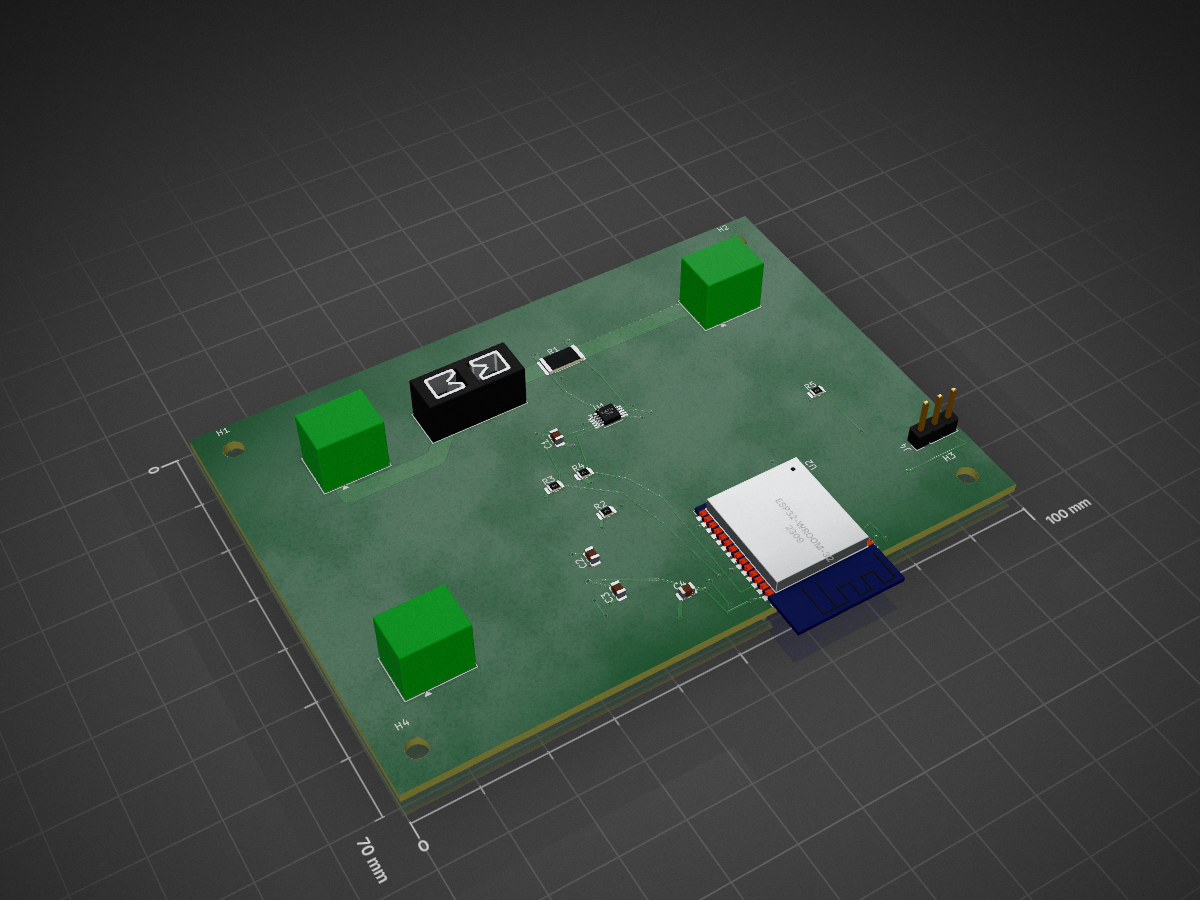
Panel node is an open-source printed circuit board by johnugbor, from the johnugbor/RoboSolar repository on GitHub, published under the MIT licence. It is a 2-layer board of 100 × 70 mm with 20 parts on 9 nets, routed with 115 tracks and 34 vias.
It is built around the ESP32-WROOM-32. Its parts include 5 resistors, 4 capacitors, 4 connectors, 2 ICs and 1 fuse. It belongs with the ESP32 boards of this library.
SKiDL-generated draft v0.1. NOT FOR FABRICATION — see blockers below.
# one-time setup (from repo root, shared with Boards 1-4)
& 'C:\Program Files\KiCad\10.0\bin\python.exe' -m venv .venv-skidl
.\.venv-skidl\Scripts\python.exe -m pip install skidl

# generate netlist + schematic, then KiCad ERC
.\.venv-skidl\Scripts\python.exe hardware\kicad\05-dock-interface\gen_schematic.py
& 'C:\Program Files\KiCad\10.0\bin\kicad-cli.exe' sch erc --output hardware\kicad\05-dock-interface\erc.rpt hardware\kicad\05-dock-interface\dock_interface.kicad_sch
Or, where make is installed (Git Bash / WSL / Linux): make kicad-board5.
Outputs: dock_interface.net, dock_interface.kicad_sch, erc.rpt.
Verified 2026-11-04: SKiDL ERC 0 errors, KiCad ERC 0 errors (17
lib_symbol_mismatch warnings — SKiDL embeds its own symbol copies; cosmetic).
The SKiDL log also prints "No footprint for PWR_FLAG" errors; PWR_FLAGs have
no footprint by design and the files are still generated.
Circuit: external 14.6V charger -> J1 -> 10mOhm shunt (INA226, 0x41; 2-3A std, 5A max) ->
spring contacts J2 (6 contacts) to the robot. D3 DECIDED 2026-11-04:
the docked robot is the I2C master for this board's INA226 over two extra
spring contacts (J2 pin4=SDA, pin5=SCL); no I2C pullups on this board -
the single 4.7k pair on Board 3 serves the bus. Dock INA226 re-strapped
0x40 -> 0x41 (A0=VS) to avoid collision with Board 3's 0x40. CHG_ALERT is
not contacted (robot polls; ALERT only on bench header J3). Contact 3 is
dock-presence sense: tied to GND here, detected by robot MCP23017
GPB6/DOCK pullup - no sense processing on dock. Refill solenoid driver is
Board 3 Sheet 5 circuit (IRLZ44N, 220R, 100k pulldown, 1N4007) on 5A fused
tap; gate arrives on J2 pin 6 (REFILL_GATE_SRC, Board 3 MCP GPA3).
Solenoid SPECIFIED (D7, 2026-11-04): 12V continuous-duty rated
(or explicitly 15V-rated) solenoid - NOT 24V (won't pull in at
12.8V). With the rail at 14.6V peak the coil would dissipate ~48%
over its 12V rating if held at 100%, so robot firmware MUST use
hit-and-hold: 100% duty for ~100ms to pull in, then 60-70%
PWM hold (coil heating scales with duty: ~0.65 x 1.48 ~= 0.96x
rated - cool). PWM comes via the MCP23017 GPA3 over I2C, so use a
low PWM rate (>=100Hz is plenty for a solenoid coil) and remember
the 100k fail-closed pulldown turns it off when undocked/idle. J3 is
bench/debug only. AprilTag mount mechanical only (BOM line, no circuit).
Generated schematic uses net labels (mode="labels", same as Boards 1-4).
dock_interface.kicad_pcb (100x70mm, 2-layer) is generated by make_pcb.py
from dock_interface.net - placement, scripted routing, bottom GND zone:
& 'C:\Program Files\KiCad\10.0\bin\python.exe' hardware\kicad\05-dock-interface\make_pcb.py
& 'C:\Program Files\KiCad\10.0\bin\kicad-cli.exe' pcb drc --output hardware\kicad\05-dock-interface\drc.rpt hardware\kicad\05-dock-interface\dock_interface.kicad_pcb
Verified 2026-11-04: KiCad DRC 0 violations, 0 unconnected pads (cleanest
board so far - not even silkscreen warnings). Render:
board5-layout-stage2.png.
Placement rationale: charge path J1 -> R1 (10mOhm shunt) -> J2 spring contacts runs short and wide (2.5mm top copper) across the north edge for the 5A max charge current. The INA226 (U1) is rotated 90 degrees so its Vin+/Vin-/Vbus pads face north and take short Kelvin taps straight off the shunt pads, while SDA/SCL/ALERT/A0 escape south, away from the charge path. LM2936 (U2) sits west next to J1. The solenoid driver (F1 5A blade fuse, Q1 IRLZ44N, D1 flyback, J4) is grouped across the south edge, its drain return on the bottom layer, well away from the INA226 front-end. Bench header J3 is on the east edge; no I2C pullups on this board (the pair lives on Board 3, per D3).
Still NOT FOR FABRICATION: blockers 2 and 5 below remain open (no reverse-current blocking on the charge path - ideal-diode ECO still to add; spring-contact mechanics/ratings are not proven by this PCB), and footprints/pinouts (INA226 MSOP-10, LM2936 SOT-223 variant, blade fuse holder, J2 contact assembly) need human peer review.
| Qty | Value | Footprint | References |
|---|---|---|---|
| 4 | MountingHole_3.2mm_M3 | MountingHole_3.2mm_M3 | H1, H2, H3, H4 |
| 3 | 4.7k | R_0805_2012Metric | R3, R4, R5 |
| 3 | Conn_01x02 | TerminalBlock_MaiXu_MX126-5.0-02P_1x02_P5.00mm | J1, J2, J3 |
| 2 | 100nF | C_0805_2012Metric | C1, C4 |
| 2 | 10uF | C_0805_2012Metric | C2, C3 |
| 1 | 10k | R_0805_2012Metric | R2 |
| 1 | 20A Blade | Fuseholder_Blade_Mini_Keystone_3568 | F1 |
| 1 | 5m 1% >=2W | R_2512_6332Metric | R1 |
| 1 | Conn_01x03 | PinHeader_1x03_P2.54mm_Vertical | J4 |
| 1 | ESP32-WROOM-32 | ESP32-WROOM-32 | U2 |
| 1 | INA226 | MSOP-10_3x3mm_P0.5mm | U1 |
It measures 100 × 70 mm and has 2 copper layers, 1.6 mm thick.
20 parts, built around the ESP32-WROOM-32. The full list of its parts is on this page, with links to each part's symbol and footprint where PCBKit's library has them.
From the johnugbor/RoboSolar repository on GitHub, at the commit this page was made from: the board is hardware/kicad/02-panel-node/panel_node.kicad_pcb and its schematic hardware/kicad/01-soiling-station/solar_soiling.kicad_sch. PCBKit opens the board in the browser, with nothing to install.
Its repository publishes it under the MIT licence: you may reuse it on that licence's terms (keep the author's notice, and for a copyleft licence share your changes alike).
johnugbor/RoboSolar
SKiDL-generated draft v0.1. NOT FOR FABRICATION — see blockers below.

johnugbor/RoboSolar
SKiDL-generated draft v0.1. NOT FOR FABRICATION — see blockers below.

johnugbor/RoboSolar
SKiDL-generated draft v0.1. NOT FOR FABRICATION — see blockers below.

johnugbor/RoboSolar
SKiDL-generated draft v0.1. NOT FOR FABRICATION — see blockers below.

asterics/esp32_mouse_keyboard
ESP32 implementation for HID over GATT Keyboard and Mouse (Bluetooth Low Energy). Including serial API for external modules (similar to Adafruit EZKey HID)


Bellafaire/ESP32-Smart-Watch
An open source smartwatch based on the ESP32 compatible with the Arduino IDE.


likeablob/slow-movie-player-7c
Yet another "Slow Movie Player" implementation with 7-color E-Paper module and ESP32.

JSnowden33/Wii-Bluetooth-Replacement
This project is a full replacement for the Nintendo Wii's Bluetooth module. Emulation of the Bluetooth module is performed on the PIC32 based on rnconrad's emulator, while controller connectivity on the ESP32 is based…