Microcontroller
Kinetoscope: A Sega Genesis Video Player
- Size
- 50.8 × 78.7 mm
- Copper layers
- 2
- Thickness
- 1.6 mm
- Parts
- 47
- Nets
- 147
- Pads
- 408
- Tracks, vias
- 1,568, 96
- Pours
- 3
- Routed
- Yes
- KiCad
- KiCad 8.0 (file 20240108)
- Created
- 27 Mar 2024
- Updated
- 9 Nov 2025
Overview
Microcontroller is an open-source printed circuit board by joeyparrish, from the joeyparrish/kinetoscope repository on GitHub, published under the MIT licence. It is a 2-layer board of 50.8 × 78.7 mm with 47 parts on 147 nets, routed with 1,568 tracks and 96 vias.
It is built around the 74LVC2G125DP, 74AHC373D and 74LVC138AD, with the 74AHC04D and 74AHC74D among its other parts. Its parts include 15 capacitors, 14 ICs, 7 resistors, 7 connectors and 2 crystals. It belongs with the retro computing and games boards of this library.
Main components
574LVC2G125DP
TSSOP-8-40℃~+125℃ 1 1.65V~5.5V 1.9ns@5V,50pF 2 32mA 32mA 4uA 74LVC Schmitt trigger Tri-State Unidirectional TSSOP-8 Buffers, Drivers, Receivers, Transceivers ROHSNexperiaBuffers, Drivers, Receivers, Transceivers74AHC373D
SO-20-300mil-40℃~+125℃ 1ns 2V~5.5V 4ns 4ns 74AHC 8 80uA D Latch Tri-State SO-20-300mil Latches ROHSNexperiaLatches74LVC138AD
-- Signal Switches, Multiplexers, Decoders ROHSNexperiaSignal Switches, Multiplexers, Decoders74AHC04D
SOIC-14-40℃~+125℃ 1 1.5V~3.85V 1.9V、2.9V、4.4V 2V~5.5V 2uA 500mV~1.65V 6 7.5ns@5V,50pF 74AHC 8mA 8mA SOIC-14 Inverters ROHSNexperiaInverters74AHC74D
SOP-14-40℃~+125℃ 1 115MHz 2 2V~5.5V 2uA 3pF 500ps 5ns 74AHC Series 8mA 8mA 9.3ns@5V,50pF Asynchronous Complementary D-Type Rising Edge Set and Reset SOP-14 Flip Flops ROHSNexperiaFlip Flops
README
hardware/README.mdKinetoscope Hardware Design
The hardware is composed of several stacking boards, each of which hosts a set of subcomponents. The subcomponents are each in a subsheet, exposing hierarchical pins and buses to the parent sheet.
One of these boards includes a microcontroller with WiFi, and runs its own
firmware to take commands from the Sega ROM. See firmware in the
../firmware/ folder.
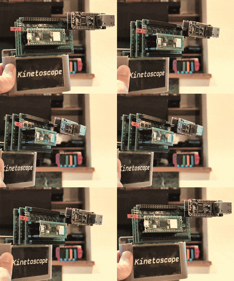
Prototype
The first working prototype looked like this:

Prerequisites
The hardware design was done in KiCad 8, and routing was done in FreeRouting. To install KiCad 8 and FreeRouting on Ubuntu, run:
sudo add-apt-repository --yes ppa:kicad/kicad-8.0-releases
sudo apt update
sudo apt install --install-recommends kicad default-jre wget unzip
wget https://github.com/freerouting/freerouting/releases/download/v1.9.0/freerouting-1.9.0-linux-x64.zip
sudo unzip -j -d /opt/freerouting freerouting-1.9.0-linux-x64.zip freerouting-1.9.0-linux-x64/lib/app/freerouting-executable.jarTo install the custom footprints and symbols used in this design, on Ubuntu run:
mkdir -p ~/.local/share/kicad/8.0
cp -a hardware/libraries/* ~/.local/share/kicad/8.0/If you have pre-existing KiCad configs, add these new symbol and footprint libraries to your config via "Preferences" > "Manage Symbol Libraries" and "Preferences" > "Manage Footprint Libraries".
If you don't have pre-existing KiCad configs, you can copy the tables used in the automated workflows:
mkdir -p ~/.config/kicad/8.0
cp .github/workflows/*-lib-table ~/.config/kicad/8.0/To see hardware schematics without KiCad, open the PDF files in the
hardware/ folder.
To order boards, see hardware zip files attached to releases. These can be uploaded to JLCPCB.
TODO: Document ordering process
Boards
The stacking boards are:
cart: Cartridge Board- This is the board that actually plugs into the Sega Genesis.
- It has 2MB of flash, which acts as the "ROM" chip for addresses 0-2MB, and contains the code that runs on the Sega.
- The flash chip is compatible with the Krikzz FlashKit Programmer MD.
- There is also a pin header on top that the other boards stack onto.
- The pin header could also be used as a kind of breakout board for the development of other Sega cartridge projects.
- Right-angle pin headers on the sides of the board are optional, and used only for debugging.
- When ordering this through JLCPCB:
- Be sure to set the following options:
- Surface Finish: ENIG
- Gold Fingers: Yes
- 30°finger chamfered: Yes
- The following parts will not be properly placed by JLCPCB's systems
automatically, and must be adjusted manually during the ordering process:
- J1 (pin header for attaching other boards, wrong location and rotation)
- U2 (voltage regulator, offset a little too far to the right)
- The following optional parts may be populated by hand if you wish:
- J4 (2-pin right-angle header for measuring current)
- Be sure to set the following options:
sram-bank: SRAM Bank Board- There are actually two of these in the stack, one for each 1MB SRAM bank.
- These host the SRAM itself, and the buffers that allow it to be alternately controlled by the Sega or the microcontroller. This is the most complex. Two solder jumpers on the board select whether it responds as bank 0 or bank 1.
- When ordering this through JLCPCB:
- The following parts could easily be populated by hand if you wish:
- J1 & J2 (stacking headers, 2x26 and 2x21 pins respectively)
- The following must be soldered by hand:
- JP1 and JP2 are solder jumpers that must be closed on each board; to set bank 0, bridge center to left on both jumpers; to set bank 1, bridge center to right on both jumpers (also indicated on silkscreen)
- The following parts could easily be populated by hand if you wish:
microcontroller: Microcontroller Board- This hosts the microcontroller, registers, sync token, and buffers to send data to SRAM.
- The registers and sync token allow the Sega to send commands to the microcontroller and wait for responses.
- The microcontroller is a Raspberry Pi Pico W, which receives commands through the registers and sync token, and is responsible for WiFi/Ethernet and streaming video to SRAM. You can buy one here for $7 (as of September 2024): https://www.adafruit.com/product/5544
- When ordering this through JLCPCB:
- The following parts may not be properly rendered by JLCPCB's systems
automatically. You may choose to leave them off your order and populate
them by hand if you wish:
- J3 and J4 are 20-pin female headers @ 0.1 inch pitch, to mount a Raspberry Pi Pico W with male headers facing down
- The following parts could easily be populated by hand if you wish:
- J1 & J2 (stacking headers, 2x26 and 2x21 pins respectively)
- J6 (optional 2x3 female header to connect to an Ethernet Adapter Board with an Adafruit Ethernet Featherwing)
- The following must be done by hand:
- A single jumper must be added to either J5 or J7 (see silkscreen notes for play vs programming setting)
- The following parts may not be properly rendered by JLCPCB's systems
automatically. You may choose to leave them off your order and populate
them by hand if you wish:
ethernet: Ethernet Adapter Board- This connects to an optional header on the microcontroller board and allows you to plug in the Adafruit Ethernet Featherwing.
- If Ethernet is connected, the firmware prefers Ethernet over WiFi.
- When ordering this through JLCPCB:
- All headers could easily be populated by hand if you wish to skip paid
assembly:
- J1 & J2 (female headers on top of the board, 1x16 and 1x12 respectively, where the Featherwing plugs in)
- The following must be done by hand, because JLCPCB will only
populate one side of the board:
- J3 (male header on the bottom of the board, where it attaches to the Microcontroller Board)
- All headers could easily be populated by hand if you wish to skip paid
assembly:
Sheets
The subsheets are:
address-counter-internal: SRAM address counter- The microcontroller doesn't have enough pins to output the SRAM address it wants to write to, so instead, this counter is used to generate sequential addresses.
buffer-16-internal: 16-bit tri-state, level-shifting buffer- This buffer allows us to manage control of the 16-bit data bus on the SRAM, switching between Sega and microcontroller control when needed.
buffer-22-internal: 22-bit tri-state, level-shifting buffer- This buffer allows us to manage control of the 19-bit address bus and control signals on the SRAM, switching between Sega and microcontroller control when needed.
data-register-internal: 16-bit serial-to-parallel shift register- The microcontroller doesn't have enough pins to output the SRAM words it wants to write, so instead, this register is used to convert a serial output from the microcontroller into the parallel input needed by the SRAM.
flash-internal: Flash connected to buses- Flash memory connected to buses to simplify top-level schematics.
kinetoscope-header-internal: Kinetoscope stacking pin headers- The stacking pin headers used for inter-board signals.
register-file-internal: 4x 8-bit Register File- Special registers the Sega writes to and the microcontroller reads from to receive commands.
sram-internal: SRAM connected to buses- SRAM connected to buses to simplify top-level schematics.
sync-token-internal: Shared Sync Token- A pair of single bit tokens. One can be set by the Sega and cleared by the microcontroller, and the other vice-versa. Both CPUs can read the state of both tokens. For the command bit, the Sega sets it to tell the microcontroller that a command has been written to the registers. The microcontroller clears it when the command has been completed. For the error bit, the microcontroller sets it to tell the Sega that an error has occurred, and the Sega clears it after the error has been read.
Routing
To reroute a PCB after modifying the schematic:
- Open the PCB in KiCad
- Select all (CTRL+A)
- Right click the board, "Select >", "Filter Selected Items..."
- Uncheck "All items"
- Check "Include tracks" and "Include vias"
- Delete (Delete key)
- Update PCB from schematic (F8)
- Click "Update PCB", then "Close"
- Save PCB (CTRL+S)
- Select "File", "Export >", "Specctra DSN..."
- Click "Save" (and "Replace" if prompted)
- Run
route-pcb.shwith the name of the board. For example:
./route-pcb.sh sram-bankAfter the routing process completes:
- Open the PCB in KiCad
- Select "File", "Import >", "Specctra Session..."
- Select the .ses file corresponding to this design
- Click "Open"
- Redo fill zones (B)
- Select "Inspect", "Design Rules Checker"
- Click "Run DRC"
- Manually fix any violations or unconnected items
Programming
To program the Flash chip in-place:
- Insert the cartridge board into the Krikzz FlashKit Programmer MD
- Write to it as you would a normal flash cart, using the original FlashKit-MD software (GUI) or FlashKit MD Python Client (command line)
Parts
47| Qty | Value | Footprint | References |
|---|---|---|---|
| 15 | 22nF | Capacitor_SMD:C_0603_1608Metric | C1, C2, C3, C4, C5, C6, C7, C8, C9, C10, C11, C14, C16, C20, C32 |
| 7 | 10k | Resistor_SMD:R_0603_1608Metric | R2, R3, R4, R5, R6, R7, R8 |
| 5 | 74LV161A | Package_SO:TSSOP-16_4.4x5mm_P0.65mm | U3, U4, U5, U6, U7 |
| 2 | 1x2 jumper right-angle | Connector_PinHeader_2.54mm:PinHeader_1x02_P2.54mm_Horizontal | J5, J7 |
| 2 | 74AHC373 | Package_SO:TSSOP-20_4.4x6.5mm_P0.65mm | U12, U14 |
| 2 | 74LV164A | Package_SO:TSSOP-14_4.4x5mm_P0.65mm | U8, U9 |
| 2 | 74LVC138A | Package_SO:TSSOP-16_4.4x5mm_P0.65mm | U15, U17 |
| 2 | ~ | Connector_PinHeader_2.54mm:PinHeader_1x20_P2.54mm_Vertical | J3, J4 |
| 2 | ~ | Jumper:SolderJumper-2_P1.3mm_Bridged_RoundedPad1.0x1.5mm | J_~{WE}_0, J_~{WE}_1 |
| 1 | 74AHC04 | Package_SO:TSSOP-14_4.4x5mm_P0.65mm | U2 |
| 1 | 74AHC74 | Package_SO:TSSOP-14_4.4x5mm_P0.65mm | U13 |
| 1 | 74LVC2G125 | Package_SO:VSSOP-8_2.3x2mm_P0.5mm | U18 |
| 1 | Conn_02x03_Odd_Even | Connector_PinHeader_2.54mm:PinHeader_2x03_P2.54mm_Vertical | J6 |
| 1 | ~ | kinetoscope-cart-header:kinetoscope-cart-board-template | X1 |
| 1 | ~ | Connector_PinHeader_2.54mm:PinHeader_2x26_P2.54mm_Vertical | J1 |
| 1 | ~ | Connector_PinHeader_2.54mm:PinHeader_2x21_P2.54mm_Vertical | J2 |
| 1 | ~ | Raspberry_Pi_Pico_W:Raspberry_Pi_Pico_W_template | X2 |
Questions
How big is the Microcontroller PCB?
It measures 50.8 × 78.7 mm and has 2 copper layers, 1.6 mm thick.
What parts does the Microcontroller use?
47 parts, built around the 74LVC2G125DP, 74AHC373D, 74LVC138AD and 74AHC04D. The full list of its parts is on this page, with links to each part's symbol and footprint where PCBKit's library has them.
Where can I download the Microcontroller KiCad files?
From the joeyparrish/kinetoscope repository on GitHub, at the commit this page was made from: the board is hardware/microcontroller.kicad_pcb and its schematic hardware/address-counter-internal.kicad_sch. PCBKit opens the board in the browser, with nothing to install.
Can I use the Microcontroller design in my own project?
Its repository publishes it under the MIT licence: you may reuse it on that licence's terms (keep the author's notice, and for a copyleft licence share your changes alike).
More from joeyparrish/kinetoscope
3- 2 layers50.8 × 78.7 mm

- 2 layers83.7 × 64.5 mm

- 2 layers24 × 45.4 mm

Similar boards
- 2 layers

- 4 layers145.5 × 89.6 mm

- 4 layers152.4 × 64.8 mm

Breakout
adrienkohlbecker/BB816
A homebrew 16 bit breadboard computer based on WDC's 65C816 processor
83 parts52 - 2 layers96 × 48 mm

- 2 layers75 × 55 mm

Wellfed bench
Isaac-Duarte/wellfed
Open firmware that runs the PETLIBRO Granary PLAF103 pet feeder on your own Wi-Fi: no cloud, no account. Early and in testing.
93 parts8MIT - 2 layers95 × 65 mm

- 2 layers50 × 87 mm

StackChanPwd
lipoyang/StackChanPwd
M5Stack-embedded super cute humanoid controller unit
47 parts6Apache-2.0 - 4 layers19.6 × 9.4 mm