2 layers354.5 × 132.5 mm
Panels001
jibonaronno/documentsA
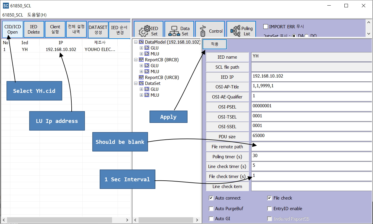
It is required to change settings using SCLManager.exe when required for new setup.
308 parts4

 jibonaronno/documentsA4
It is required to change settings using SCLManager.exe when required for new setup.
Extension is an open-source printed circuit board by jibonaronno, from the jibonaronno/documentsA repository on GitHub. It is a 2-layer board of 45.7 × 38.1 mm with 8 parts on 8 nets, routed with 62 tracks and 6 vias.
Its parts include 5 connectors, 2 capacitors and 1 IC.
SA_Client.ini has following configs:
LocalIp=192.168.10.105
...
...
PATH=D:/develop/MZAutomation/SAProgram/ClientProc_2017_Dev_NoTimer_Minsu/ClientProc/61850_CFG/CFG/61850/SA_CFG
SAVE_PATH =D:/develop/MZAutomation/SAProgram/ClientProc_2017_Dev_NoTimer_Minsu/ClientProc/61850_CFG/LOG/61850
ENG_PATH =D:/develop/MZAutomation/SAProgram/ClientProc_2017_Dev_NoTimer_Minsu/ClientProc/61850_CFG/DB/ied_info_gw.csv
These configurations should be changed if machine or location is changed.
It is required to change settings using SCLManager.exe when required for new setup.
Confluence Pages From PDA ACQ Operation and calculation / Integration of various current values Copy of 차단기 동작 특성 페이지 https://jlee193.atlassian.net/wiki/spaces/PDA/pages/514129921/Copy+of
Bushing Documentation Page From PDA 부싱 누설 전류 페이지 https://jlee193.atlassian.net/wiki/spaces/PDA/pages/296812597
An Initial Concept of hardware pptx file downloaded in Confluence folder 종합예방진단시스템(20210625)_HW팀.pptx 하드웨어 구성 https://jlee193.atlassian.net/wiki/spaces/PDA/pages/154042616
| Qty | Value | Footprint | References |
|---|---|---|---|
| 4 | Screw | wago_smd_2screw:WAGO_2060-452_998-404 | J2, J3, J4, J5 |
| 2 | 100n | Capacitor_SMD:C_0603_1608Metric | C1, C2 |
| 1 | 2.0 mm SMD Socket | Connector_PinSocket_2.00mm:PinSocket_2x04_P2.00mm_Vertical_SMD | J1 |
| 1 | AMS1117 5.0 | Package_TO_SOT_SMD:SOT-223-3_TabPin2 | U1 |
jibonaronno/documentsA
It is required to change settings using SCLManager.exe when required for new setup.

jibonaronno/documentsA
It is required to change settings using SCLManager.exe when required for new setup.

jibonaronno/documentsA
It is required to change settings using SCLManager.exe when required for new setup.

jibonaronno/documentsA
It is required to change settings using SCLManager.exe when required for new setup.

jibonaronno/documentsA
It is required to change settings using SCLManager.exe when required for new setup.

jibonaronno/documentsA
It is required to change settings using SCLManager.exe when required for new setup.

jibonaronno/documentsA
It is required to change settings using SCLManager.exe when required for new setup.

jibonaronno/documentsA
It is required to change settings using SCLManager.exe when required for new setup.

jibonaronno/documentsA
It is required to change settings using SCLManager.exe when required for new setup.

jibonaronno/documentsA
It is required to change settings using SCLManager.exe when required for new setup.

jibonaronno/documentsA
It is required to change settings using SCLManager.exe when required for new setup.

jibonaronno/documentsA
It is required to change settings using SCLManager.exe when required for new setup.


joeycastillo/Sensor-Watch
A board replacement for the classic Casio F-91W wristwatch

rusefi/rusefi
rusefi - GPL internal combustion engine control unit

hoglet67/RGBtoHDMI
Bare-metal Raspberry Pi project that provides pixel-perfect sampling of Retro Computer RGB/YUV video and conversion to HDMI

shanteacontrols/OpenDeck
A platform for building interactive control and sensing devices using MIDI and OSC built with Zephyr RTOS.

hackclub/OnBoard
💡 Join 1,000 teenagers and make your first PCB with a $100 grant!

dangiu/PicoMemcard
Emulating PSX Memory Card (or controller) using a Raspberry Pi Pico

OLIMEX/DIY-LAPTOP
Do It Yourself Open Source Hardware and Software Modular Hacker's Friendly Laptop
It measures 45.7 × 38.1 mm and has 2 copper layers, 1.6 mm thick.
8 parts. The full list of its parts is on this page, with links to each part's symbol and footprint where PCBKit's library has them.
From the jibonaronno/documentsA repository on GitHub, at the commit this page was made from: the board is uprojects/Tommi Savikko/extension/extension.kicad_pcb. PCBKit opens the board in the browser, with nothing to install.
Its repository states no licence, so its author keeps all rights: ask jibonaronno before reusing the design.