4 layers91 × 52 mm
Filament dryer monitor
alessandrocardelli/filament-dryer-monitor
ESP32 controller for eSUN eBOX Lite. main is the non-heating SAFE BRING-UP reference; its heater output remains locked OFF.
110 parts

 jericho-adler/ocean-harness
An ADAS CAN interposer for the Fisker Ocean, designed in KiCad. It plugs in between the car's harness and the ADAS ECU's main connector (CON1), so a comma device can sit between the car and the ECU.
Ocean harness is an open-source printed circuit board by jericho-adler, from the jericho-adler/ocean-harness repository on GitHub, published under the CERN-OHL-S-2.0 licence. It is a 4-layer board of 89 × 72.2 mm with 33 parts on 72 nets, routed with 357 tracks and 64 vias.
It is built around the DG419LEDY-T1-GE4, PESD1CAN,215-ES and ESR03EZPJ121, with the SMAJ16A, CC0603KRX7R9BB104 and TCC0603X7R334K500CT among its other parts. Its parts include 10 diodes, 5 resistors, 5 connectors, 3 capacitors and 2 ICs.


An ADAS CAN interposer for the Fisker Ocean, designed in KiCad. It plugs in between the car's harness and the ADAS ECU's main connector (CON1), so a comma device can sit between the car and the ECU. When the board has no power it drops back to a plain hard-wired passthrough, and the car behaves exactly as stock.
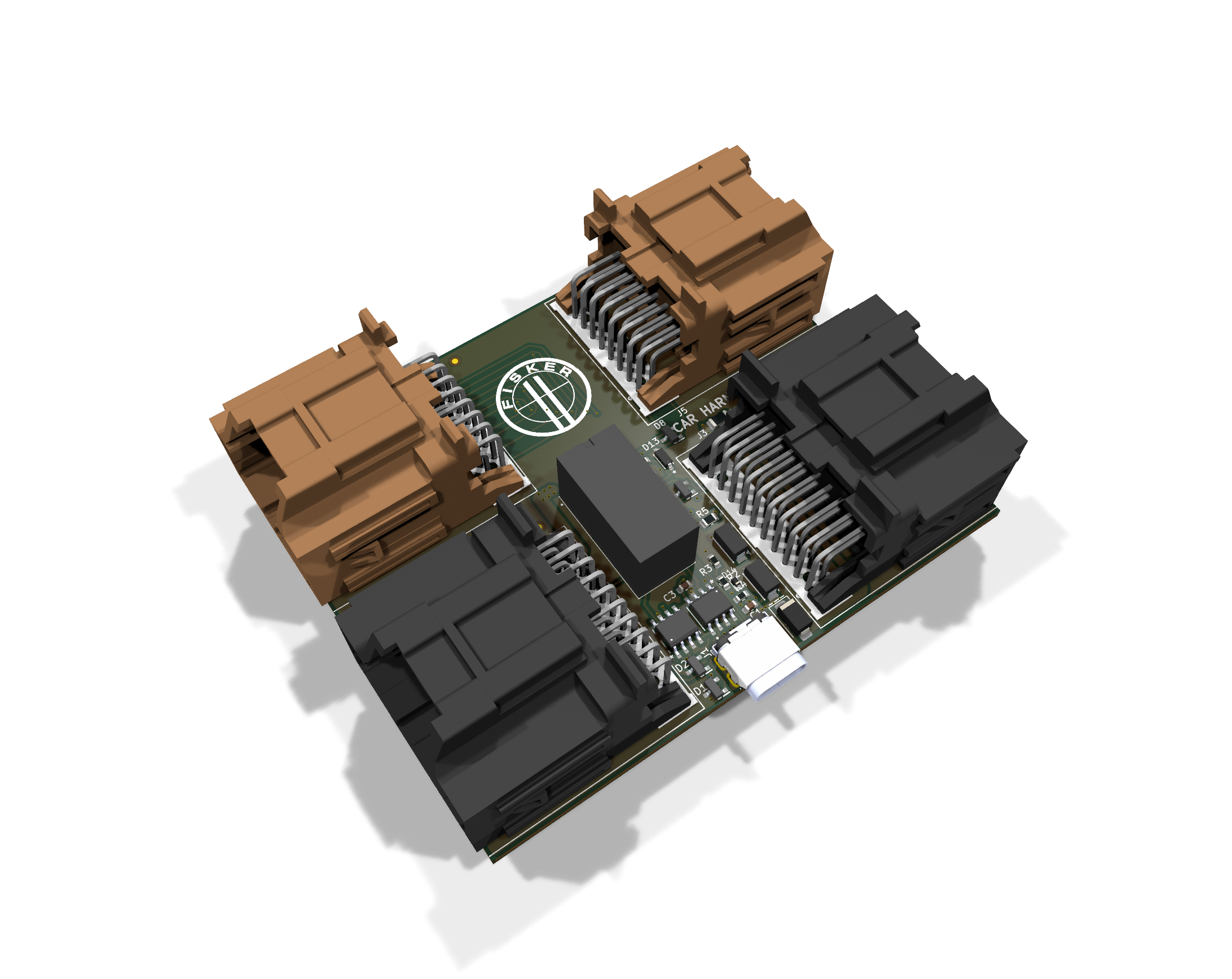
| Board | 89.0 × 72.2 mm, 4 layers, every part on the top side |
| Parts | 28 components, plus two M3 mounting holes and three fiducials |
| Mounting | One M3 hole in each gap between the stacked headers |
| Power | Taken from the harness VBAT on J3 pin 1. No external supply |
| Comma link | USB-C (J1) carrying 12 V and CAN, comma "OBD-C" style. It's not a USB data port |
| Revision | Rev 2, November 2026. New layout, not yet built |
| Ref | Part | Side | Carries |
|---|---|---|---|
| J3 | Molex 0346910200, 20-way | Vehicle harness | CON1 section A |
| J5 | Molex 0346910162, 16-way | Vehicle harness | CON1 section B |
| J4 | Molex 0346910200, 20-way | ADAS ECU | CON1 section A |
| J6 | Molex 0346910162, 16-way | ADAS ECU | CON1 section B |
| J1 | JAE DX07S024XJ1R1100, USB-C | Comma device | 12 V, three CAN pairs, one control line |
The harness side is on the right edge ("CAR HARNESS-->") and the ECU side is on the left ("<--ADAS ECU"). 22 of the 36 CON1 circuits are carried. Every other pin is left unconnected.
VBAT comes in on J3 pin 1. It goes straight through to J4 pin 1 (1.6 mm leaving J3, 2.4 mm along B.Cu, 2.0 mm into J4, with six 0.4 mm vias at the layer change), so the ECU keeps its own supply whatever the board is doing.
The board takes its own power from the same feed through F1 (Bel 0685T3000-01, 3 A time-lag, 63 V), so a short anywhere on the board side opens F1 rather than the car's fuse for the ECU. VBAT_FUSED then goes to D10 (SS34 Schottky), which blocks reverse polarity into the 12V_PROT rail, D9 and D11 (two SMAJ16A) clamp transients on it, and C1 decouples it. 12V_PROT powers the comma device through all four USB-C VBUS pins.
R5 (160 Ω) drops about 2 V from 12V_PROT to make VIN, which runs the relay coil. That holds the coil near its 12 V rating on a 14 V running rail. CR1 (1N4148W) is the coil's flyback diode, and C2 decouples VIN.
The analog switches get their own clamped supply. VIN runs through D12 (DSK14) and R6 (3.3 kΩ) to SW_VCC, where D13 (BZT52C12) holds it to about 12 V and C3 decouples it. SW_VCC feeds both V+ and VL on U1 and U2. This clamp is the one used on the Volvo/Polestar harness box, and rev 2 added it for three reasons:
VIN through the switches' internal clamp diodes when the board is unpowered but the car bus is live.K1 (Omron G5V-2-H1 DC12, DPDT) switches the vehicle's ADAS CAN (HSCAN1, J3 pins 19/20). Its common contacts are on the vehicle side and its normally-closed contacts go to the ECU, so with no power the car and ECU are hard-wired together and the comma device is out of the loop.
Once the board has power, the relay moves the vehicle side over to the comma device's _C pair (J1 A2/A3). The ECU stays wired to the device's _MOD pair (J1 B2/B3), so the device has the car on one port and the ECU on the other. The coil is energized the whole time the board has power. The -H1 variant is used for its 150 mW coil (against 500 mW for the standard part) and its 21.6 V maximum coil voltage.
U1 and U2 (Vishay DG419LE SPDT analog switches) decide what happens between the two segments. The comma device controls them through SBU 1 on J1 A8.
With SBU 1 low, the switches bridge _C to _MOD, so the car and ECU stay connected and the device only listens. That's the default: R2 + R3 form a 240 Ω pulldown, so it's also the safe state if the device never drives the pin.
With SBU 1 high, the bridge opens and R4 (120 Ω) is switched across the ECU-side pair, so that segment keeps its own termination. The device is now fully in the middle.
| Power | SBU 1 | Car ↔ ECU | Comma device |
|---|---|---|---|
| Off | Any | Connected through K1's normally-closed contacts | Isolated |
| On | Low | Connected through U1/U2 | Listening on both segments |
| On | High | Cut. The ECU segment is terminated by R4 | In the middle |
These run between the harness and ECU connectors untouched:
The mid-range radar CAN (MRR) also passes straight through. It has a passive stub tap to J1 A10/A11 so the device can monitor it.
Four PESD1CAN ESD arrays protect:
_C pair (J1 A2/A3), next to J1D14 (PESD24VS1UB) protects SBU 1. The reserved COMMA_P/COMMA_N pair has no ESD diode now that D1 has moved.
F1 fuses the board's tap off VBAT. Reverse polarity and transients on the supply are handled by D10, D9 and D11 as described above.
| Pin | USB-C name | Signal | Use |
|---|---|---|---|
| A4, A9, B4, B9 | VBUS | 12V_PROT | 12 V supply to the device |
| A1, A12, B1, B12, shell | GND | GND | |
| A2 / A3 | TX1+ / TX1- | ADAS_CAN_H_C / ADAS_CAN_L_C | Car side of the intercepted ADAS CAN, live when the relay is energized |
| B2 / B3 | TX2+ / TX2- | ADAS_CAN_H_MOD / ADAS_CAN_L_MOD | ECU side of the intercepted ADAS CAN |
| A11 / A10 | RX2+ / RX2- | MRR_CAN_H / MRR_CAN_L | Listen-only tap on the mid-range radar CAN |
| B11 / B10 | RX1+ / RX1- | COMMA_P / COMMA_N | Wired only to J1. Reserved |
| A8 | SBU1 | SBU 1 | Switch control input |
| A5, B5, A6, A7, B6, B7, B8 | CC, D+/D-, SBU2 | Not connected |
| Pin | Signal | Path |
|---|---|---|
| 1 | VBAT (Harness_12v) | Straight through, and powers the board through F1 and D10 |
| 6 | USS2_PWR | Straight through |
| 7 | USS1_PWR | Straight through |
| 14 | GND | Straight through, and board ground |
| 15 | USS1_PWR_N | Straight through |
| 16 | USS1_Signal | Straight through |
| 17 | USS2_Signal | Straight through |
| 18 | USS2_PWR_N | Straight through |
| 19 / 20 | ADAS CAN L / H | Intercepted through K1. ADAS_CAN on J3, ADAS_CAN_MOD on J4 |
| Pin | Signal | Path |
|---|---|---|
| 1 / 9 | MRR CAN L / H | Straight through, tapped to J1 A10/A11 |
| 2 / 3 | CMRR FR CAN H / L | Straight through |
| 4 / 5 | CMRR RR CAN H / L | Straight through |
| 10 / 11 | CMRR FL CAN H / L | Straight through |
| 12 / 13 | CMRR RL CAN H / L | Straight through |
| 15 / 16 | DMS LED1 L / H | Straight through |
| Layer | Use |
|---|---|
| F.Cu | Signals, GND pour |
| In1.Cu | Solid GND plane |
| In2.Cu | VIN plane, with a 12V_PROT island under J1, C1 and D9 to D11 |
| B.Cu | Signals, GND pour |
The two header pairs face out of opposite edges, so the J5↔J6 pin order is reversed. Those 12 nets cross over in the strip between the headers. The six ultrasonic lines run on B.Cu around J4. Signal tracks are 0.25 mm with 45° bends. The VBAT passthrough leaves J3 on B.Cu at 1.6 mm (squeezed between the J3 mounting peg and the board edge), runs up the right side and across the top at 2.4 mm, and drops to F.Cu through six 0.4 mm vias for the last 2.0 mm run into J4. F1 sits in the gap between J5 and J3 and is fed from that trunk through three vias. VBAT_FUSED runs back down to D10 on a 1.2 mm F.Cu track, under J3 and clear of its keepouts. The 12 V path to the USB-C runs on an F.Cu bar from D10/D11 to C1, then through the In2 island. The island connects solid to the VBUS pins.
| Path | Contents |
|---|---|
PCB Files/ | KiCad 10 project (.kicad_pro, .kicad_sch, .kicad_pcb) and design reviews |
images/ | Iso render |
3D models/ | STEP model. Still shows the rev 1 layout |
| Rev | Date | Changes |
|---|---|---|
| 2 | November 2026 | Added the DG419 supply clamp (D12, R6, D13, C3); U1/U2 V+ and VL now come from it. Added F1 on the VBAT tap, moved D1 to the _C pair, added D14 on SBU 1, widened the ECU VBAT passthrough, and put a "12V, COMMA ONLY" note on the back silkscreen under J1. Board shrunk from 115.75 × 75.25 mm to 89.0 × 72.2 mm with every part on top. M3 holes moved into the header gaps. Re-routed, silkscreen redone |
| 1 | October 2026 | First layout. Reviewed in PCB Files/design_review_2026-10-13.md |
The rev 1 design review still covers the circuit, but the rev 2 layout hasn't had its own review.
MFG Part # fields now match their real parts.)Licensed under the CERN Open Hardware Licence Version 2 - Strongly Reciprocal (CERN-OHL-S-2.0).
This is a community hardware design shared as-is, with no warranty. It's designed for the Fisker Ocean only, and using it on other platforms is unverified. Use at your own risk.
| Qty | Value | Footprint | References |
|---|---|---|---|
| 4 | PESD1CAN | My_Components:PESD1CAN | D1, D2, D3, D8 |
| 3 | 120 | My_Components:Rohm ESR03EZPJ121 | R2, R3, R4 |
| 3 | Fiducial_1mm_Mask2mm | Fiducial:Fiducial_1mm_Mask2mm | FID1, FID2, FID3 |
| 2 | Molex 0346910162 | My_Components:CONN_SD-34691-100_16_MOL | J5, J6 |
| 2 | Molex 0346910200 | My_Components:CONN_SD-34691-100_20_MOL | J3, J4 |
| 2 | MountingHole_3.2mm_M3 | MountingHole_3.2mm_M3 | H1, H2 |
| 2 | SMAJ16A | My_Components:SMAJ16A | D9, D11 |
| 2 | Vishay DG419LEDY-T1-GE4 | My_Components:Vishay DG419LEDY-T1-GE4 | U1, U2 |
| 1 | 0.1uF | Capacitor_SMD:C_0603_1608Metric | C2 |
| 1 | 0.33uF | Capacitor_SMD:C_0603_1608Metric | C1 |
| 1 | 100nF | Capacitor_SMD:C_0603_1608Metric | C3 |
| 1 | 160 | Resistor_SMD:R_0805_2012Metric | R5 |
| 1 | 1N4148W-7-F | Footprints:SOD123_DIO | CR1 |
| 1 | 3.3K | My_Components:Rohm ESR03EZPJ121 | R6 |
| 1 | 3A | Fuse:Fuse_1206_3216Metric | F1 |
| 1 | BZT52C12 | Footprints:SOD123_DIO | D13 |
| 1 | DSK14 | Diode_SMD:D_SOD-123F | D12 |
| 1 | G5V-2-H1 DC12 | My_Components:Omron G5V-2-DC12 | K1 |
| 1 | JAE DX07S024XJ1R1100 | My_Components:JAE DX07S024XJ1R1100 | J1 |
| 1 | MBRA340T3G | Diode_SMD:D_SMA | D10 |
| 1 | PESD24VS1UB | Diode_SMD:D_SOD-523 | D14 |
alessandrocardelli/filament-dryer-monitor
ESP32 controller for eSUN eBOX Lite. main is the non-heating SAFE BRING-UP reference; its heater output remains locked OFF.

NOAA-PMEL/ASVCO2
Open Source Repository for the Autonomous Surface Vehicle CO2 (ASVCO2) gen2 system


chilly23/PCBGolf-master-Comma.ai
Compact PCB studies for the comma.ai PCBGolf challenge, including KiCad and EasyEDA designs, BOMs, STEP models, and routing-status reports.

cubicap/usb4-thing
An attemt at creating a USB4 multiplexer controlled by ESP32-S3.


MotorDynamicsLab/Leviathan
Leviathan Main Controller for Voron 2 / Trident 3D Printers
It measures 89 × 72.2 mm and has 4 copper layers, 1.62 mm thick.
33 parts, built around the DG419LEDY-T1-GE4, PESD1CAN,215-ES, ESR03EZPJ121 and SMAJ16A. The full list of its parts is on this page, with links to each part's symbol and footprint where PCBKit's library has them.
From the jericho-adler/ocean-harness repository on GitHub, at the commit this page was made from: the board is PCB Files/Ocean Harness.kicad_pcb and its schematic PCB Files/Ocean Harness.kicad_sch. PCBKit opens the board in the browser, with nothing to install.
Its repository publishes it under the CERN-OHL-S-2.0 licence: you may reuse it on that licence's terms (keep the author's notice, and for a copyleft licence share your changes alike).