
4 layers36 × 39 mm
 jay-waghmare/MachXO2-KiCad-Board1
Custom MachXO2 FPGA Development Board - KiCad Design - Power, Clock, JTAG, LEDs - By Jay Waghmare
MACHXO2 test is an open-source printed circuit board by jay-waghmare, from the jay-waghmare/MachXO2-KiCad-Board repository on GitHub, published under the MIT licence. It is a 4-layer board of 65 × 48 mm with 52 parts on 138 nets, routed with 641 tracks and 175 vias.
It is built around the LCMXO2-640HC-6MG132I, FT231XQ-R and USBLC6-2SC6, with the 1N5819HW among its other parts. Its parts include 24 capacitors, 13 resistors, 5 ICs, 5 connectors and 4 diodes. It belongs with the fPGA and programmable logic boards and the FPGA and CPLD boards of this library.


Custom breakout board for Lattice LCMXO2-640HC-6MG132I - Designed in KiCad 9.0.3 - 8 Sheets Hierarchical - By Jay Waghmare



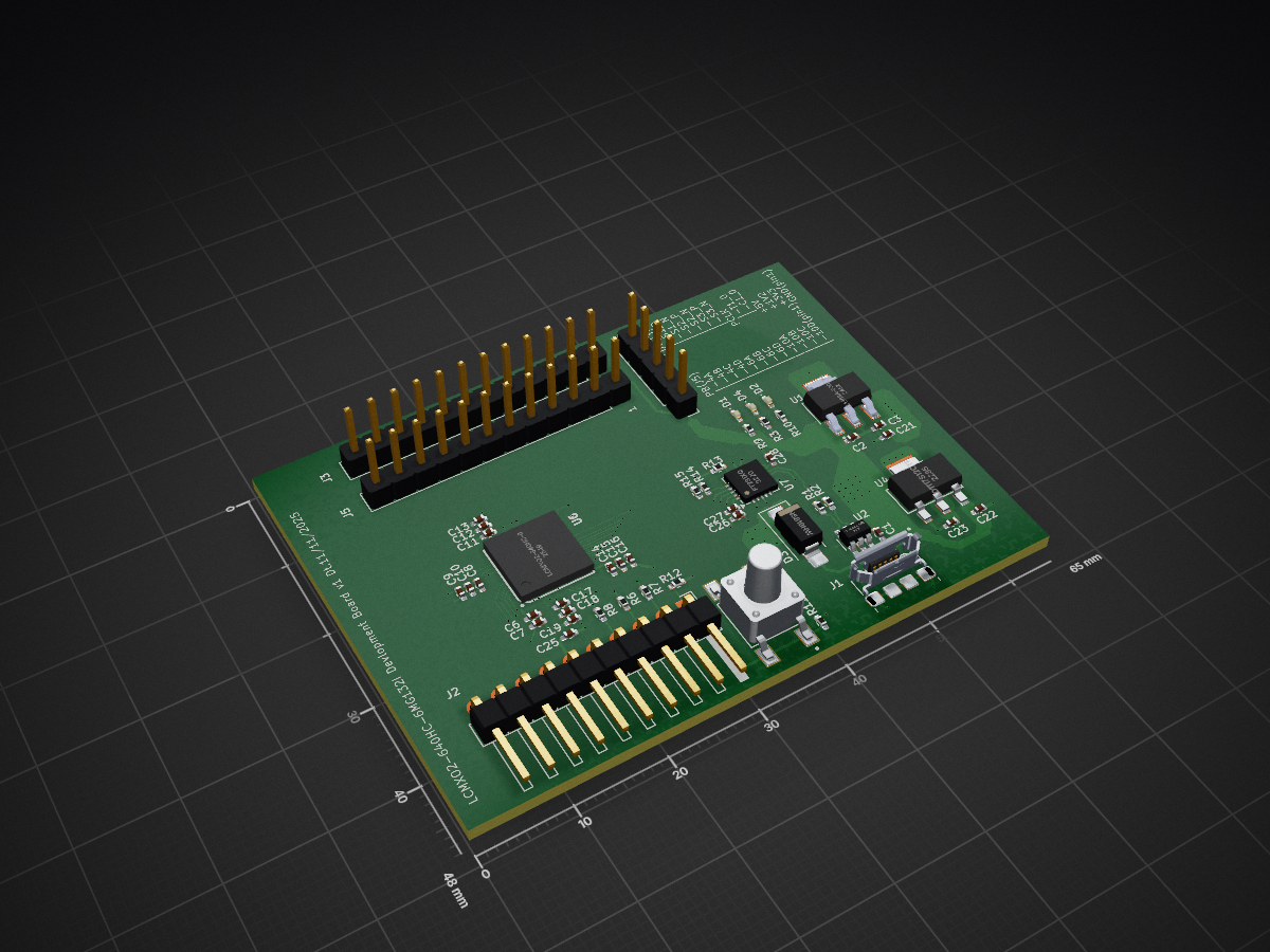
3D Render - MachXO2-640HC Board (KiCad 3D View)
Custom FPGA development board designed from scratch in KiCad for Lattice MachXO2 LCMXO2-640HC-6MG132I (640 LUTs, 132-ball CSBGA).
Full breakout board, not simple LED:
Why I made my own? To learn FPGA hardware - Power sequencing, decoupling, JTAG, I/O banks.
8 Sheets Hierarchical (KiCad 9.0.3, file MACHXO2_test.kicad_sch):
| Sheet | File | Content |
|---|---|---|
| 1/8 | MACHXO2_test.kicad_sch | Top Level - Power, User_IO/Banks, Device_Management blocks |
| 2/8 | Power.kicad_sch | Power: USB Mini, 3.3V/1.2V LDOs, FPGA VCC/VCCIO decoupling C6 0.1uF C7 4.7uF etc, VCCIO table |
| 3/8 | USER_IO_Bank_T | Bank0 Top - U6B LCMXO2 Bank0, JTAG TDO/TDI/TCK/TMS, J3 12-pin socket |
| 4/8 | USER_IO_Bank_R | Bank1 Right - U6C Bank1, LVDS1/2/3, PCLK, J4 10-pin header |
| 5/8 | USER_IO_Bank_L | Bank Left - U6D Bank Left PL2A...PL7B |
| 6/8 | USER_IO_Bank_B | Bank Bottom - U6E Bank Bottom PB4A...PB14B |
| 7/8 | USER_Config | Config - JTAG J2, PROGRAMN button SW1, FT231XQ UART, JTAG header flywire table |
| 8/8 | GND&NC | GND & NC - U6F/U6G NC pins and GND balls |
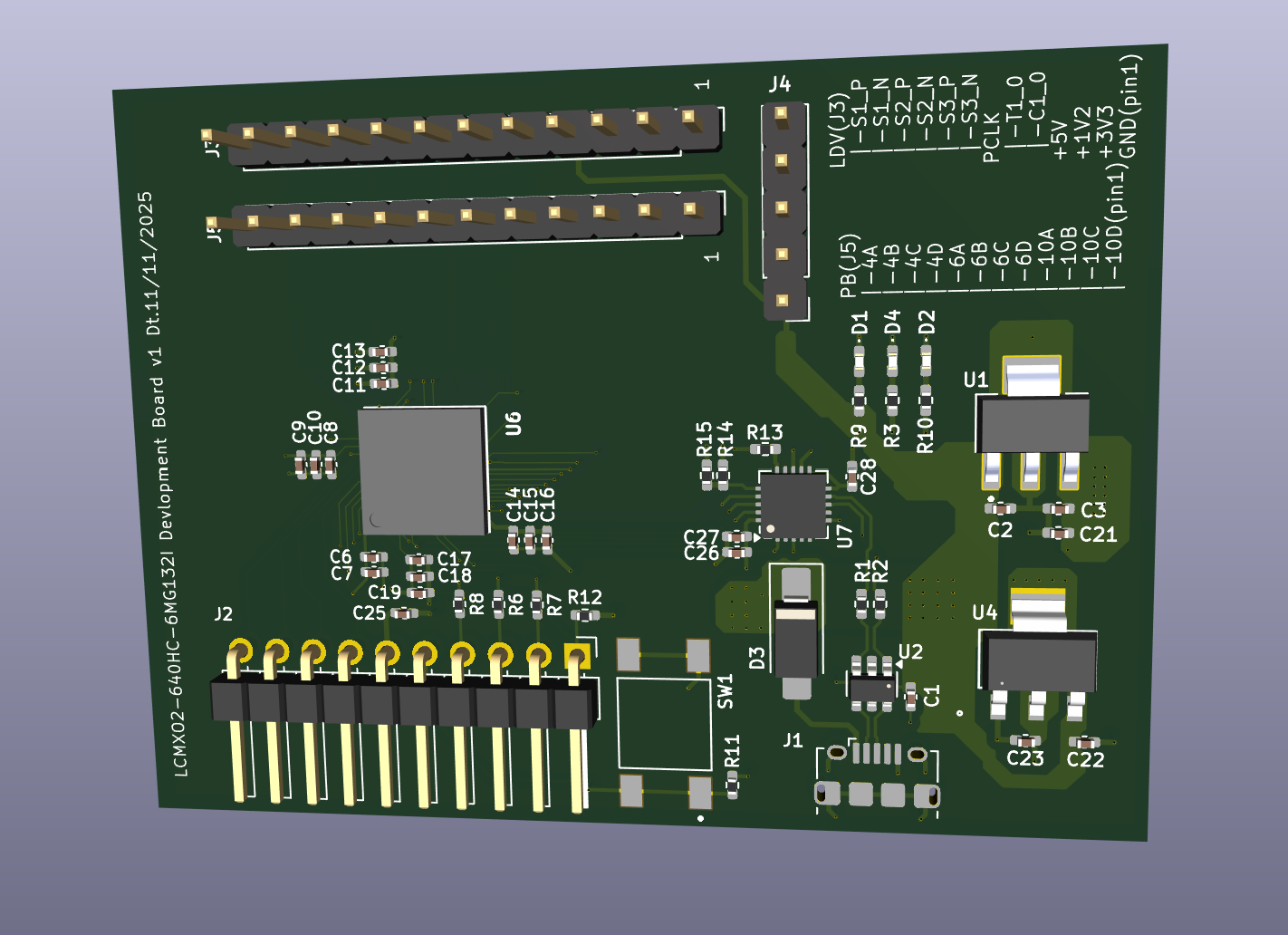
You uploaded: .kicad_pro, .kicad_sch, .kicad_pcb, .kicad_prl, schematic.pdf, 3d-render.png, pcb_preview.png - Full project!
| Schematic PDF | PCB Preview | 3D Render |
|---|---|---|
| schematic.pdf (8 pages) | 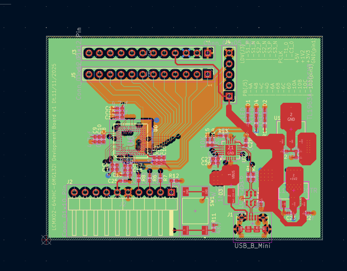 | 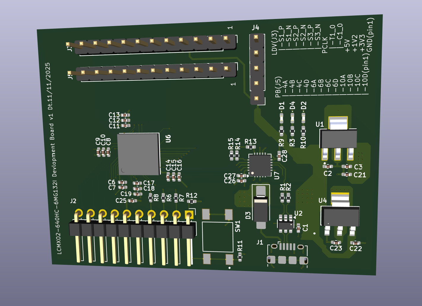 |
MACHXO2_test.kicad_pro → Schematic Editor (8 sheets) → PCB Editor → 3D ViewJay Waghmare - FPGA
If you like FPGA hardware boards, please ⭐ star!
MIT License
Designed from scratch in KiCad 9.0.3
| Qty | Value | Footprint | References |
|---|---|---|---|
| 9 | 0.1uf | Capacitor_SMD:C_0402_1005Metric_Pad0.74x0.62mm_HandSolder | C1, C6, C8, C11, C14, C17, C25, C27, C28 |
| 8 | 4.7uf | Capacitor_SMD:C_0402_1005Metric_Pad0.74x0.62mm_HandSolder | C2, C7, C9, C13, C16, C19, C22, C26 |
| 5 | 22R | Resistor_SMD:R_0402_1005Metric_Pad0.72x0.64mm_HandSolder | R1, R2, R6, R7, R8 |
| 4 | 1uf | Capacitor_SMD:C_0402_1005Metric_Pad0.74x0.62mm_HandSolder | C10, C12, C15, C18 |
| 3 | 10uf | Capacitor_SMD:C_0402_1005Metric_Pad0.74x0.62mm_HandSolder | C3, C21, C23 |
| 3 | 1K | Resistor_SMD:R_0402_1005Metric_Pad0.72x0.64mm_HandSolder | R3, R9, R10 |
| 3 | 4K7 | Resistor_SMD:R_0402_1005Metric_Pad0.72x0.64mm_HandSolder | R11, R12, R14 |
| 3 | LED | LED_SMD:LED_0402_1005Metric_Pad0.77x0.64mm_HandSolder | D1, D2, D4 |
| 2 | 10K | Resistor_SMD:R_0402_1005Metric_Pad0.72x0.64mm_HandSolder | R13, R15 |
| 2 | Conn_01x12_Pin | Connector_PinHeader_2.54mm:PinHeader_1x12_P2.54mm_Vertical | J3, J5 |
| 1 | 1N5819HW | Diode_SMD:D_SMA_Handsoldering | D3 |
| 1 | Conn_01x05_Pin | Connector_PinHeader_2.54mm:PinHeader_1x05_P2.54mm_Vertical | J4 |
| 1 | Conn_01x10_Pin | Connector_PinHeader_2.54mm:PinHeader_1x10_P2.54mm_Horizontal | J2 |
| 1 | FT231XQ | Package_DFN_QFN:QFN-20-1EP_4x4mm_P0.5mm_EP2.5x2.5mm | U7 |
| 1 | LCMXO2-640HC-6MG132I | CSBG132:BGA132C50P14X14_800X800X135 | U6 |
| 1 | LD1117S12CTR | LD1117S12CTR:SOT-223_STM | U4 |
| 1 | SW_Push_Dual | TL3301AF160QG:SW_TL3301AF160QG | SW1 |
| 1 | TL1963A-33DCYR | TL1963A-33DCYR:VREG_TL1963A-33DCYR | U1 |
| 1 | USBLC6-2SC6 | Package_TO_SOT_SMD:SOT-23-6 | U2 |
| 1 | USB_B_Mini | Connector_USB:USB_Micro-B_Amphenol_10118194-0001LF_Horizontal | J1 |


ThunderFly-aerospace/TFUSBSERIAL01
USB-C to serial converter with Pixhawk telemetry JST-GH connector


It measures 65 × 48 mm and has 4 copper layers, 1.6 mm thick.
52 parts, built around the LCMXO2-640HC-6MG132I, FT231XQ-R, USBLC6-2SC6 and 1N5819HW. The full list of its parts is on this page, with links to each part's symbol and footprint where PCBKit's library has them.
From the jay-waghmare/MachXO2-KiCad-Board repository on GitHub, at the commit this page was made from: the board is MACHXO2_test.kicad_pcb and its schematic MACHXO2_test.kicad_sch. PCBKit opens the board in the browser, with nothing to install.
Its repository publishes it under the MIT licence: you may reuse it on that licence's terms (keep the author's notice, and for a copyleft licence share your changes alike).