2 layers60 × 50 mm

 IslamHUFE/rp2040
RP design with rp2040
Rp2040 is an open-source printed circuit board by IslamHUFE, from the IslamHUFE/rp2040 repository on GitHub, published under the MIT licence. It is a 4-layer board of 48.1 × 41.6 mm with 33 parts on 56 nets, routed with 427 tracks and 135 vias.
It is built around the RP2040, W25Q128JVSIQ and TPD4E05U06DQAR, with the ABM8-272-T3 among its other parts. Its parts include 16 capacitors, 7 resistors, 4 ICs, 4 connectors and 1 crystal. It belongs with the RP2040 boards of this library.


A custom development board built around the Raspberry Pi RP2040 microcontroller.
This project is a personal PCB design exercise based on the official RP2040 hardware-design reference material. The goal was to translate the reference design into a complete, organized KiCad project and develop a practical DevKit-style board around the RP2040.
Project status: PCB design / hardware development
The board was designed from the RP2040 reference design with attention to the complete hardware implementation rather than treating the microcontroller as a standalone component. The repository contains the KiCad schematic and PCB layout, supporting component data, manufacturing-related outputs, and visualizations of the finished board.
The design includes the supporting circuitry required around the RP2040, including its clocking and other core hardware, while keeping the board in a compact development-kit form suitable for experimentation and further firmware development.
The main hardware design is provided as a KiCad project:
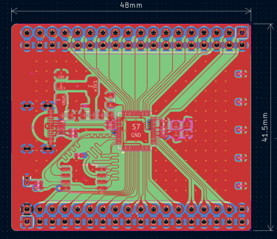
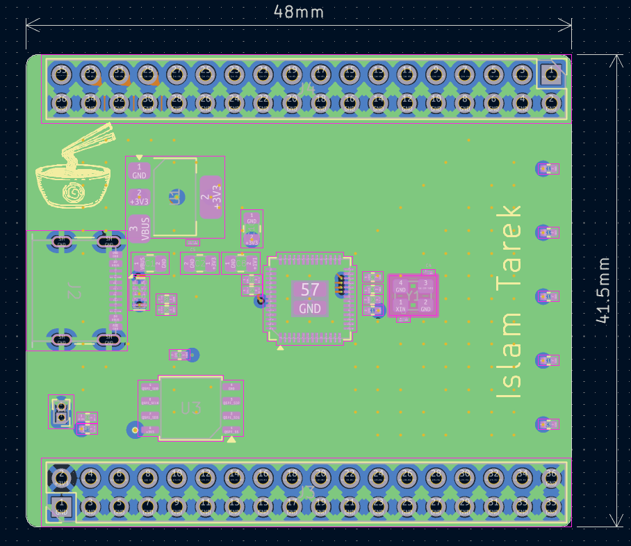
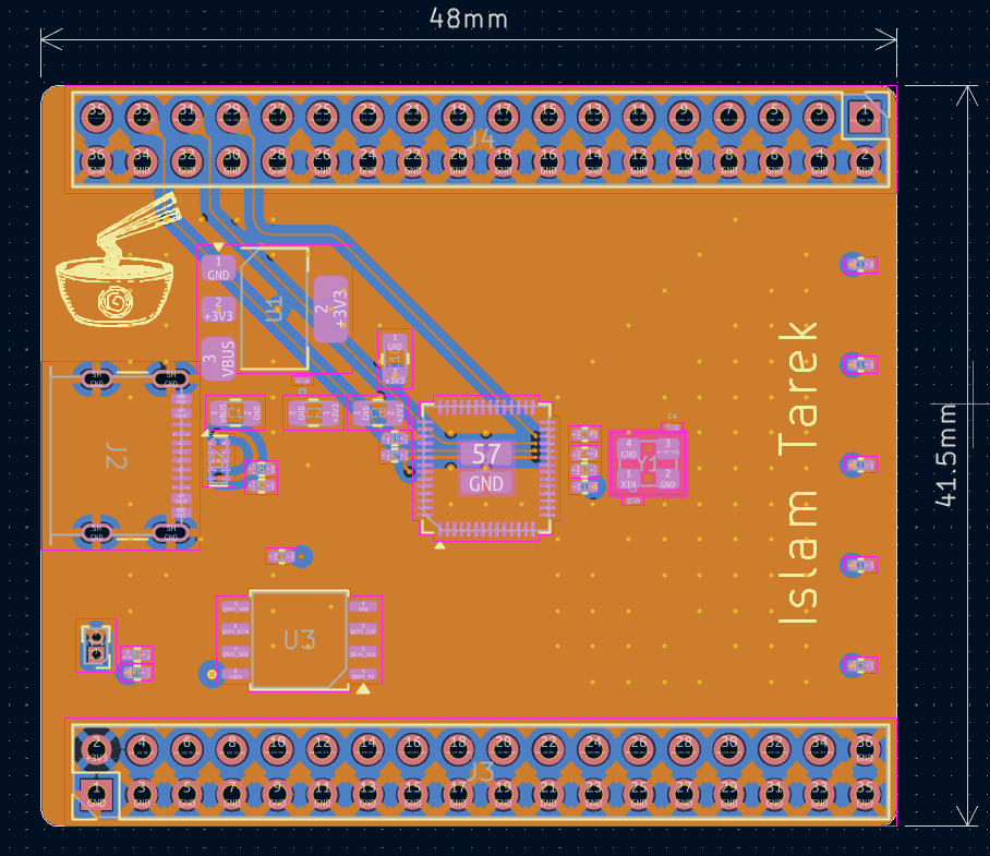
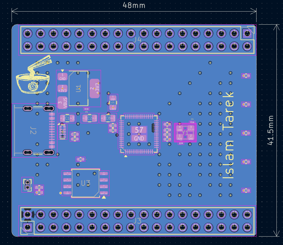
RS/RS.kicad_sch — SchematicRS/RS.kicad_pcb — PCB layoutRS/RS.kicad_pro — KiCad project fileRS/RS.pdf — Schematic/documentation exportRS/bom/ — Bill of Materials and related outputsRS/hi.pretty/ — Custom KiCad footprints used by the project3D/ — Additional 3D component model filesref/ — Reference material used during the design processThe following renders show the PCB layer-by-layer, followed by a combined view of the complete board stack.
The first layer of the PCB, showing the routing and copper features placed on the top side of the board.
The second PCB layer, showing the corresponding internal copper features and routing.
The third layer of the four-layer PCB stack, providing additional routing and copper area within the board.
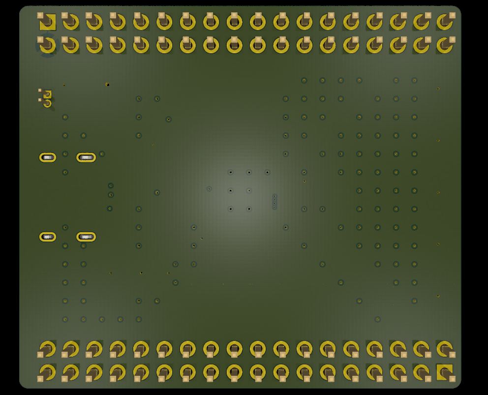
The final layer of the PCB stack, showing the copper features on the bottom side of the board.
All four PCB layers displayed together to give an overall view of the board's routing density and layer organization.
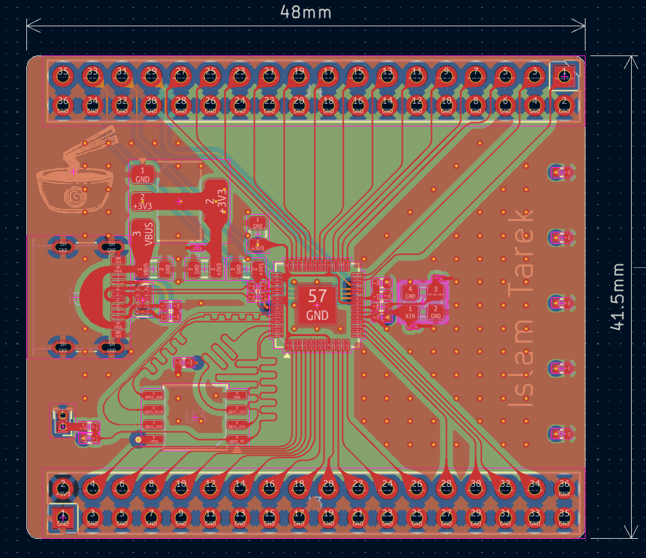
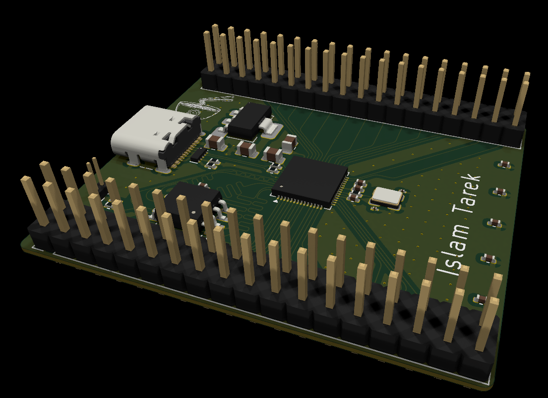
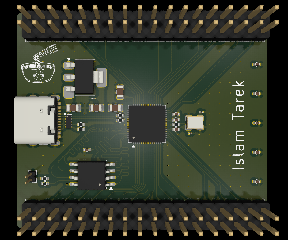
The following renders show the completed PCB from different perspectives. They provide a more intuitive view of the board outline, component placement, connectors, and overall physical arrangement.
A perspective view of the assembled PCB, highlighting the component placement and overall board geometry.
A second perspective of the board showing the physical arrangement from a different angle.
A final 3D overview of the DevKit, showing the complete board design as a physical assembly.
The board was developed by studying the RP2040 hardware reference design and adapting its requirements into a custom PCB workflow:
The design was developed with the RP2040 hardware design documentation as a primary reference. The relevant reference material is included in the ref/ directory for reproducibility and study.
This repository represents a custom hardware implementation and learning project. It is based on the RP2040 reference design, but the PCB, schematic organization, component selection, and physical layout were developed as part of this project.
The design should be reviewed and electrically validated before being used as a production board.
Designed by Islam Tarek Moawad
| Qty | Value | Footprint | References |
|---|---|---|---|
| 9 | 100n | Capacitor_SMD:C_0402_1005Metric | C6, C7, C9, C11, C12, C13, C14, C15, C16 |
| 2 | 10u | Capacitor_SMD:C_0805_2012Metric | C1, C2 |
| 2 | 15p | Capacitor_SMD:C_01005_0402Metric | C3, C4 |
| 2 | 1k | Resistor_SMD:R_0402_1005Metric | R3, R4 |
| 2 | 1u | Capacitor_SMD:C_0805_2012Metric | C8, C10 |
| 2 | 27 | Resistor_SMD:R_0402_1005Metric | R6, R7 |
| 2 | 5.1k | Resistor_SMD:R_0402_1005Metric | R1, R2 |
| 2 | Conn_02x18_Odd_Even | Connector_PinHeader_2.54mm:PinHeader_2x18_P2.54mm_Vertical | J3, J4 |
| 1 | 100n | Capacitor_SMD:C_01005_0402Metric | C5 |
| 1 | ABM8-272-T3 | Crystal:Crystal_SMD_Abracon_ABM8G-4Pin_3.2x2.5mm | Y1 |
| 1 | Conn_01x02_Pin | Connector_PinHeader_1.00mm:PinHeader_1x02_P1.00mm_Vertical | J1 |
| 1 | DNF | Resistor_SMD:R_0402_1005Metric | R5 |
| 1 | LOGO | hi:noodles | G*** |
| 1 | NCP1117-1.5_SOT223 | Package_TO_SOT_SMD:SOT-223-3_TabPin2 | U1 |
| 1 | RP2040 | Package_DFN_QFN:QFN-56-1EP_7x7mm_P0.4mm_EP3.2x3.2mm | U4 |
| 1 | TPD4E05U06DQA | Package_SON:USON-10_2.5x1.0mm_P0.5mm | U2 |
| 1 | USB_C_Receptacle_USB2.0_16P | Connector_USB:USB_C_Receptacle_GCT_USB4105-xx-A_16P_TopMnt_Horizontal | J2 |
| 1 | W25Q128JVS | Package_SO:SOIC-8_5.3x5.3mm_P1.27mm | U3 |

hazy2go/gb-link-usb
Game Boy (DMG) link port to USB-C PC adapter: printer emulation, PC link, online link play. Sister project of the WiFi Game Boy cart.


open-ephys/commutator-controller
Open Ephys commutator PCB and firmware


It measures 48.1 × 41.6 mm and has 4 copper layers, 0.61 mm thick.
33 parts, built around the RP2040, W25Q128JVSIQ, TPD4E05U06DQAR and ABM8-272-T3. The full list of its parts is on this page, with links to each part's symbol and footprint where PCBKit's library has them.
From the IslamHUFE/rp2040 repository on GitHub, at the commit this page was made from: the board is RS/RS.kicad_pcb and its schematic RS/RS.kicad_sch. PCBKit opens the board in the browser, with nothing to install.
Its repository publishes it under the MIT licence: you may reuse it on that licence's terms (keep the author's notice, and for a copyleft licence share your changes alike).