2 layers86 × 31 mm

 inoa-io/satellite2
Satellite Hardware Project and Documentation
Development board is an open-source printed circuit board by inoa-io, from the inoa-io/satellite repository on GitHub, published under the CERN-OHL-P-2.0 licence. It is a 2-layer board of 153 × 77 mm with 103 parts on 157 nets, routed with 496 tracks and 2 vias.
It is built around the MAX3486CSA+, LTV-817S and SN74CBT16292DL, with the FT2232HL, LD1117S33 and BAV303-TR among its other parts. Its parts include 40 resistors, 17 capacitors, 11 diodes, 10 connectors and 8 ICs. It belongs with the microcontroller boards boards of this library.


The Inoa Satellite is a lightweight and secure gateway for your fuse box or industrial environment.
Please see our Project Pages for details.
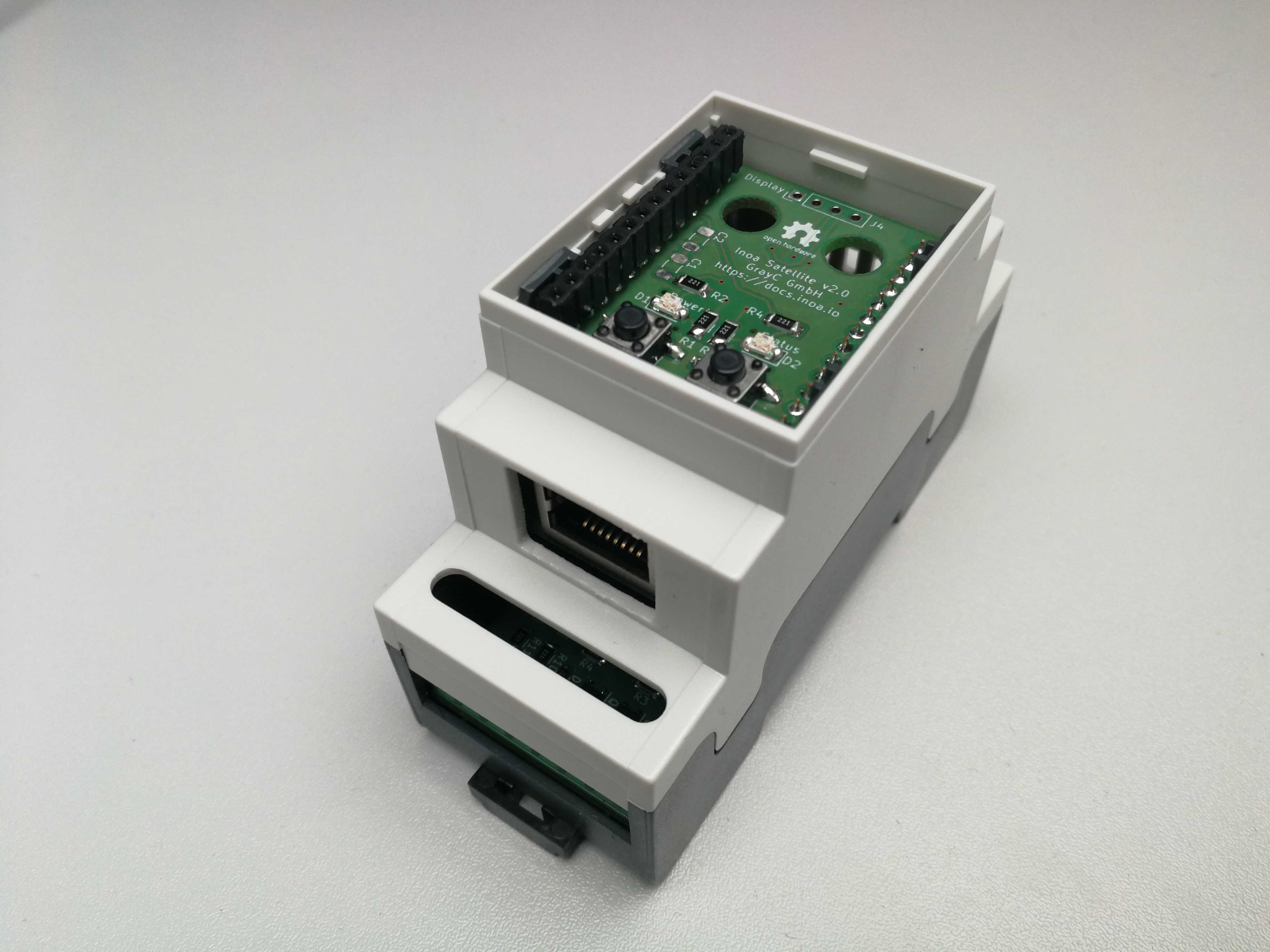
There is a huge amount of IoT gateways out there, but none of these fulfill completely all of our design goals:
We use KiCad for our PCB designs, Parts Community and SnapEDA for symbols, footprints, models 'n stuff...
To meet our design goals, we decided to:
The Satellite comes with a stacked design allowing to interchange the modules on each level of the stack to fit the needs of its planned duty.
This allows quick and cheap adjustment of single devices, ensures expandability, keeps costs low and offers replacement of defect modules with spare parts.
The Satellite consists of up to 4 levels (level 1 is the bottom). Level 3 is an optional level and may be left out.
The electric metering module is dedicated to be used for interacting with electric meters, inverters, batteries and so on. It is a base module on level 1 of the stack. Its features are:
The CT module is dedicated to be used for EMS use cases. Current transformers (split core) with voltage output may be used (e.g. SCT-013).
It is a base module on level 1 of the stack. Its features are:
The M-Bus module is dedicated to be used for interacting with different meters via RS485 or M-Bus. The module acts as M-Bus master, but a separate power supply is needed. Because the size of this power supply depends on the amount of connected meters, we decided to give the ability to choose a fitting, external power supply.
The M-Bus module is a base module on level 1 of the stack. Its features are:
The SoC module is the heart of the satellite and home of the microprocessor, flash memory and HSM (hardware security module). It is the main module on level 2 of the stack. Its features are:
The Ethernet module connects the Satellite to Ethernet. It is a network module on level 3 of the stack. Its features are:
Coming soon
Coming soon
The panel module is the "user interface" and home of all user input output devices of the Satellite. It is the top module on level 4. Its features are:
We use a DIN rail mounted casing in 2 FE width. See Datasheet for details.
You will need:
Clone this project and run ./build.sh. You will get a selection of the possible modules to be built. Tests will be executed and the build result is placed in the out folder.
| Folder | Purpose |
|---|---|
| ./casing | Construction files for the casing |
| ./configs | KiCad-Export configuration |
| ./development-board | Design for the development board |
| ./docs | Documentation |
| ./ethernet-extension | Design for the Ethernet module |
| ./libraries | Electric symbols, footprints and 3D models |
| ./metering-module | Design for the metering module |
| ./nbiot-extension | Design for the NB IoT module |
| ./out | Build output folder |
| ./panel-module | Design for the panel module |
| ./soc-module | Design for the SoC module |
| Serial | Module / Part | Current Version |
|---|---|---|
| SR-SC-XXX | SoC Module | v2.0 |
| SR-EM-XXX | Electric Metering | v2.0 |
| SR-CM-XXX | Current Loop Metering | v2.0 |
| SR-MM-XXX | MBus / WMBus Metering | v2.0 |
| SR-ET-XXX | Ethernet Module | v2.0 |
| SR-NB-XXX | NB IoT Module | v2.0 |
| SR-LR-XXX | LoRa / LoRa WAN Module | v2.0 |
| SR-PN-XXX | Panel Module | v2.0 |
Despite of the low energy consumption of the MCU itself, we are planning with a maximum current of 1A to be future proof for extra extensions that have a higher energy demand (LoRa, NB IoT, ...).
We chose two different of track widths for main power and for data lines (0.25 mm / 0.5 mm) and planned a minimum temperature of 0°C. See the table below.
| Track (mm) | Track (mil) | 10° | 20° | 30° | 40° | 50° | 60° |
|---|---|---|---|---|---|---|---|
| 0.1mm | 4mil | 0.4A | 0.6A | 0.8A | 0.9A | 1.0A | 1.1A |
| 0.2mm | 8mil | 0.7A | 1.0A | 1.2A | 1.4A | 1.6A | 1.7A |
| 0.3mm | 12mil | 0.9A | 1.3A | 1.6A | 1.8A | 2.0A | 2.2A |
| 0.4mm | 16mil | 1.1A | 1.5A | 1.9A | 2.2A | 2.4A | 2.7A |
| 0.5mm | 20mil | 1.3A | 1.8A | 2.2A | 2.5A | 2.8A | 3.1A |
| 0.6mm | 24mil | 1.4A | 2.0A | 2.4A | 2.8A | 3.1A | 3.4A |
We chose a 0.1mm grid for all PCB designs, because our casings and mechanics are also measured in millimeters.
We chose 0.8mm 0.4mm vias.
| Pin ESP | Pin Satellite | Pin Name | Standard Purpose |
|---|---|---|---|
| 1 | East 1 | GND | Ground |
| 2 | West 1 | 3V3 | Power supply |
| 3 | West 2 | EN3 | Reset |
| 4 | West 3 | I36 | I2C Interrupt |
| 5 | West 4 | I39 | UART 1 RX |
| 6 | West 5 | I34 | SPI 2 MISO |
| 7 | West 6 | I35 | UART 2 RX |
| 8 | West 7 | IO32 | SPI 2 MOSI |
| 9 | West 8 | IO33 | SPI 2 CLK |
| 10 | West 9 | IO25 | UART 1 TXE |
| 11 | West 10 | IO26 | UART 1 TX |
| 12 | West 11 | IO27 | SPI 2 CS (Ethernet) |
| 13 | West 12 | IO14 | Ethernet Reset |
| 14 | West 13 | IO12 | |
| 15 | NC | GND | Ground |
| 16 | West 14 | IO13 | Status LED |
| 17 | NC | NC | Internal Flash / RAM |
| 18 | NC | NC | Internal Flash / RAM |
| 19 | NC | NC | Internal Flash / RAM |
| 20 | NC | NC | Internal Flash / RAM |
| 21 | NC | NC | Internal Flash / RAM |
| 22 | NC | NC | Internal Flash / RAM |
| 23 | East 13 | IO15 | UART 2 TX |
| 24 | East 12 | IO2 | UART 2 TXE |
| 25 | East 11 | IO0 | Setup Button |
| 26 | East 10 | IO4 | Ethernet Interrupt |
| 27 | NC | NC | Internal Flash / RAM |
| 28 | NC | NC | Internal Flash / RAM |
| 29 | East 9 | IO5 | SPI 1 CS (SD) |
| 30 | East 8 | IO18 | SPI 1 CLK |
| 31 | East 7 | IO19 | SPI 1 MISO |
| 32 | NC | NC | Internal Flash / RAM |
| 33 | East 6 | IO21 | I2C SDA |
| 34 | East 5 | URXD0 | UART 0 RX |
| 35 | East 4 | UTXD0 | UART 0 TX |
| 36 | East 3 | IO22 | I2C SCL |
| 37 | East 2 | IO23 | SPI 1 MOSI |
| 38 | East 1 | GND | Ground |
| NC | East 14 | Shield | Shield / PE |
| Qty | Value | Footprint | References |
|---|---|---|---|
| 8 | 10k | Resistor_SMD:R_1206_3216Metric_Pad1.30x1.75mm_HandSolder | R4, R5, R7, R25, R34, R35, R36, R37 |
| 8 | 220R | Resistor_SMD:R_1206_3216Metric_Pad1.30x1.75mm_HandSolder | R26, R27, R28, R29, R30, R31, R32, R33 |
| 7 | 100nF | Capacitor_SMD:C_1206_3216Metric_Pad1.33x1.80mm_HandSolder | C1, C3, C4, C14, C15, C16, C17 |
| 4 | 120R | Resistor_SMD:R_1206_3216Metric_Pad1.30x1.75mm_HandSolder | R13, R14, R15, R16 |
| 4 | 2k | Resistor_SMD:R_1206_3216Metric_Pad1.30x1.75mm_HandSolder | R9, R10, R11, R12 |
| 4 | MountingHole_Pad | MountingHole:MountingHole_3.2mm_M3_DIN965_Pad | H1, H2, H3, H4 |
| 3 | 33R | Resistor_SMD:R_1206_3216Metric_Pad1.30x1.75mm_HandSolder | R1, R2, R3 |
| 3 | 400R | Resistor_SMD:R_1206_3216Metric_Pad1.30x1.75mm_HandSolder | R19, R21, R23 |
| 3 | 800R | Resistor_SMD:R_1206_3216Metric_Pad1.30x1.75mm_HandSolder | R20, R22, R24 |
| 3 | D_TVS | Diode_SMD:D_0603_1608Metric_Pad1.05x0.95mm_HandSolder | D9, D10, D11 |
| 2 | 0u1 | Capacitor_SMD:C_1206_3216Metric_Pad1.33x1.80mm_HandSolder | C11, C13 |
| 2 | 12pF | Capacitor_SMD:C_1206_3216Metric_Pad1.33x1.80mm_HandSolder | C8, C9 |
| 2 | 1k@100MHz | Resistor_SMD:R_1206_3216Metric_Pad1.30x1.75mm_HandSolder | FB1, FB2 |
| 2 | 4u7 | Capacitor_SMD:C_1206_3216Metric_Pad1.33x1.80mm_HandSolder | C10, C12 |
| 2 | BAV303 | Diode_SMD:D_MicroMELF | D4, D5 |
| 2 | C | Capacitor_SMD:C_1206_3216Metric_Pad1.33x1.80mm_HandSolder | C6, C7 |
| 2 | LTV-817S | Package_DIP:SMDIP-4_W9.53mm | U4, U5 |
| 2 | MMBT3904 | Package_TO_SOT_SMD:SOT-23 | Q1, Q2 |
| 2 | R | Resistor_SMD:R_1206_3216Metric_Pad1.30x1.75mm_HandSolder | R39, R40 |
| 2 | S8050 | Package_TO_SOT_SMD:SOT-23 | Q3, Q4 |
| 2 | SN74CBT16292 | Package_SO:TSSOP-20_4.4x6.5mm_P0.65mm | U7, U8 |
| 1 | 0R | Resistor_SMD:R_1206_3216Metric_Pad1.30x1.75mm_HandSolder | R8 |
| 1 | 10uF | Capacitor_SMD:C_1206_3216Metric_Pad1.33x1.80mm_HandSolder | C5 |
| 1 | 10uF | Capacitor_Tantalum_SMD:CP_EIA-3216-18_Kemet-A_Pad1.58x1.35mm_HandSolder | C2 |
| 1 | 12MHz | Crystal:Crystal_SMD_HC49-SD_HandSoldering | Y1 |
| 1 | 12k | Resistor_SMD:R_1206_3216Metric_Pad1.30x1.75mm_HandSolder | R38 |
| 1 | 150R | Resistor_SMD:R_1206_3216Metric_Pad1.30x1.75mm_HandSolder | R17 |
| 1 | 1N5819 | Diode_SMD:D_SOD-323_HandSoldering | D2 |
| 1 | 270R | Resistor_SMD:R_1206_3216Metric_Pad1.30x1.75mm_HandSolder | R18 |
| 1 | 2k2 | Resistor_SMD:R_1206_3216Metric_Pad1.30x1.75mm_HandSolder | R6 |
| 1 | 6V/800mA | Fuse:Fuse_1206_3216Metric_Pad1.42x1.75mm_HandSolder | F1 |
| 1 | 93C46-WMN6TP | Package_SO:SOIC-8_3.9x4.9mm_P1.27mm | U3 |
| 1 | Antenna | MountingHole:MountingHole_5.5mm | H6 |
| 1 | Antenna Cable | MountingHole:MountingHole_5.5mm | H5 |
| 1 | Audio | footprints:CUI_SJ1-3523N | J6 |
| 1 | BZT52C6V2 | Diode_SMD:D_SOD-323_HandSoldering | D1 |
| 1 | East | Connector_PinHeader_2.54mm:PinHeader_1x14_P2.54mm_Vertical | J1 |
| 1 | Ext_5V | Connector_PinHeader_2.54mm:PinHeader_1x02_P2.54mm_Horizontal | J10 |
| 1 | FT2232HL | Package_QFP:LQFP-64_10x10mm_P0.5mm | U2 |
| 1 | Keyboard | footprints:TE_5749180-1 | J4 |
| 1 | LD1117S33 | Package_TO_SOT_SMD:SOT-223-3_TabPin2 | U1 |
| 1 | MAX3486 | Package_SO:SOIC-8_3.9x4.9mm_P1.27mm | U6 |
| 1 | Mouse | footprints:TE_5749180-1 | J5 |
| 1 | PinOut | Connector_PinHeader_2.54mm:PinHeader_2x14_P2.54mm_Vertical | J9 |
| 1 | Power | LED_SMD:LED_1206_3216Metric_Pad1.42x1.75mm_HandSolder | D3 |
| 1 | Power | Button_Switch_THT:SW_E-Switch_EG1224_SPDT_Angled | SW3 |
| 1 | RXD | LED_SMD:LED_1206_3216Metric_Pad1.42x1.75mm_HandSolder | D7 |
| 1 | Reset | Button_Switch_SMD:SW_SPST_PTS645 | SW1 |
| 1 | Screw_Terminal | footprints:TE_1-1776113-0 | J2 |
| 1 | Setup | Button_Switch_SMD:SW_SPST_PTS645 | SW2 |
| 1 | Status | LED_SMD:LED_1206_3216Metric_Pad1.42x1.75mm_HandSolder | D8 |
| 1 | TXD | LED_SMD:LED_1206_3216Metric_Pad1.42x1.75mm_HandSolder | D6 |
| 1 | USB_B | Connector_USB:USB_B_OST_USB-B1HSxx_Horizontal | J3 |
| 1 | VGA | footprints:AMPHENOL_L77HDE15SD1CH4F | J7 |
| 1 | West | Connector_PinHeader_2.54mm:PinHeader_1x14_P2.54mm_Vertical | J8 |

inoa-io/satellite
Satellite Hardware Project and Documentation

inoa-io/satellite
Satellite Hardware Project and Documentation


inoa-io/satellite
Satellite Hardware Project and Documentation

inoa-io/satellite
Satellite Hardware Project and Documentation


jdg511/567Terror
Software simulation of the Glitchwave 567 (LM567 glitch pedal) — JUCE Standalone + VST3


mohamed1920said/STARTUP
KiCad 10 carrier board for the AMR central gateway firmware. The board accepts an ESP32-S3-DevKitC-1-N8R8, adds a soldered RFM95W 868 MHz radio, protected sensor interfaces, regulated 7-18 V input, an enclosure-button…

sire234/VatPoeToUsb
Ein Gerät, das über ein Ethernet-Kabel mit PoE (IEEE 802.3af) gespeist wird und an einem USB-A-Host-Port ein HID-Gerät (Tastatur, Barcode-Scanner, Maus) betreibt. Die HID-Daten stellt die Firmware über Ethernet bereit.

KozaMateusz/TemperatureManagementGUI
Graphical user interface to controll the temperature in a chamber.

Muriukidavid/esp-jtag
A JTAG programmer for esp targets based on esp-prog redone in KiCad


max-verem/stm32_ltc_encoder
STM32 based SMPTE Linear Timecode Generator/Reader, isolated input/output
It measures 153 × 77 mm and has 2 copper layers, 1.6 mm thick.
103 parts, built around the MAX3486CSA+, LTV-817S, SN74CBT16292DL and FT2232HL. The full list of its parts is on this page, with links to each part's symbol and footprint where PCBKit's library has them.
From the inoa-io/satellite repository on GitHub, at the commit this page was made from: the board is electrics/pc-board/development-board.kicad_pcb and its schematic electrics/ct-module/ct-module.kicad_sch. PCBKit opens the board in the browser, with nothing to install.
Its repository publishes it under the CERN-OHL-P-2.0 licence: you may reuse it on that licence's terms (keep the author's notice, and for a copyleft licence share your changes alike).