Skip to the content
PCBKitNew board
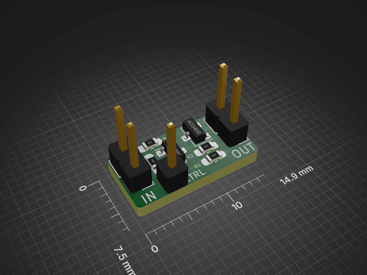
2 layers14.9 × 7.5 mmPowerSwitch, the printed circuit board in 3D

INAV I2C IO Expander board offers 8 digital outputs.

Size
14.9 × 7.5 mm
Copper layers
2
Thickness
1.6 mm
Parts
10
Nets
7
Pads
19
Tracks, vias
27, 25
Pours
1
Routed
Yes
KiCad
KiCad 5 (file 20171130)
Created
18 Jul 2019
Updated
27 Sep 2021

Overview

PowerSwitch is an open-source printed circuit board by iNavFlight, from the iNavFlight/hardware repository on GitHub. It is a 2-layer board of 14.9 × 7.5 mm with 10 parts on 7 nets, routed with 27 tracks and 25 vias.

It is built around the AO3400 and AO3401. Its parts include 4 resistors, 3 connectors and 2 transistors.
Main components

2

README

IO Expander/README.md

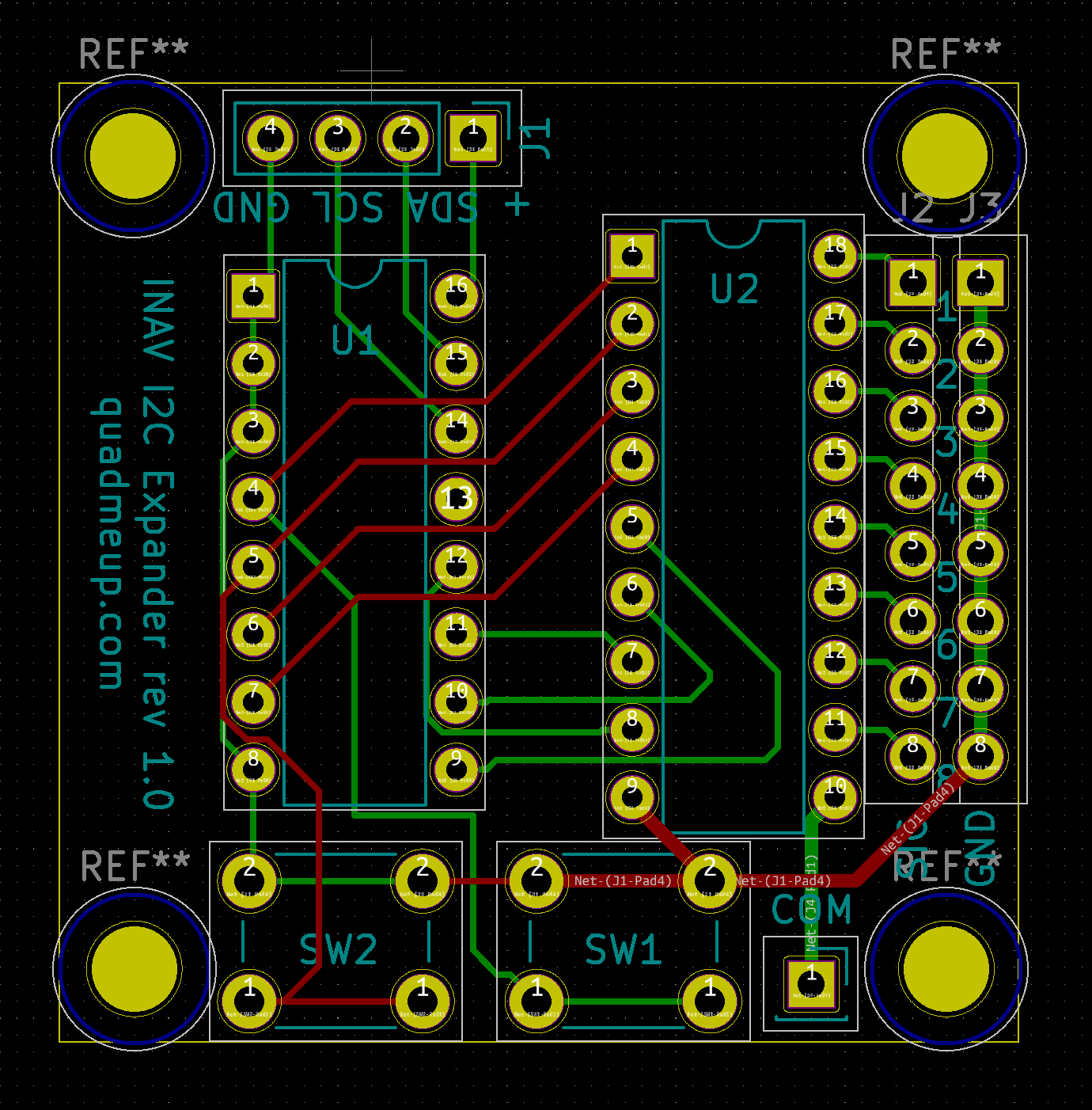
INAV I2C IO Expander board

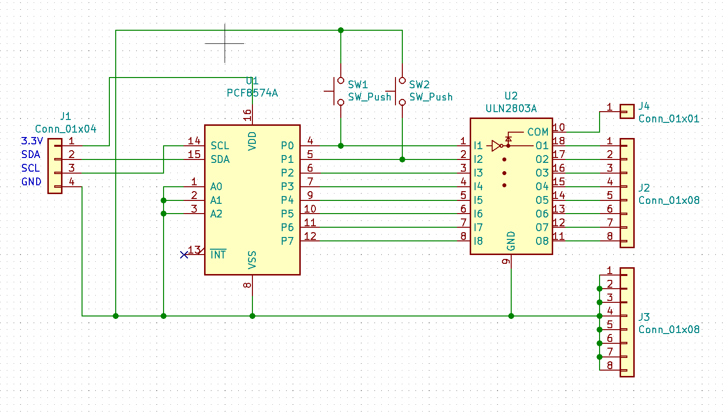
Diagram

PCB

INAV I2C IO Expander board offers 8 digital outputs.
  • All elements are THT for easy soldering by beginners
  • 36x36mm PCB with 30.5x30.5mm mounting holes fits on top of most flight controllers
  • Each channel can be loaded to around 300mA on 3.3V
  • Switching is done on the low side
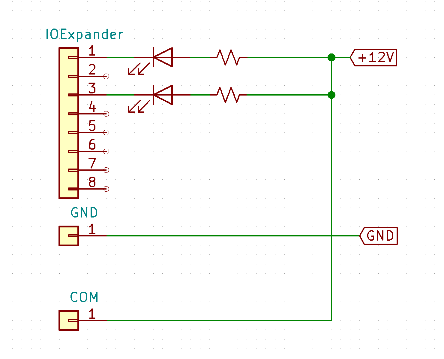
  • In case of inductive load, COM port has to be connected to the Vcc
  • Max voltage ULN2803 can handle is 50V. It is 8S ready, however 12-16V is recommended
  • Connects via I2C to any INAV compatible flight controller
  • Supported in INAV 2.6 via Logic Conditions in Programming Framework
  • Buttons are not yet supported by INAV

Example usage

Example

BOM

  • 1x PCF8574 THT
  • 1x ULN2803A THT
  • 2x Tactile button

PCB can be ordered via OSH Park

Parts

10
QtyValueFootprintReferences
26k8Resistor_SMD:R_0603_1608Metric_Pad1.05x0.95mm_HandSolderR1, R3
1PowerSwitch:LOGO_INAVLOGO
110kResistor_SMD:R_0603_1608Metric_Pad1.05x0.95mm_HandSolderR4
147kResistor_SMD:R_0603_1608Metric_Pad1.05x0.95mm_HandSolderR2
1AO3400Package_TO_SOT_SMD:SOT-23Q1
1AO3401Package_TO_SOT_SMD:SOT-23Q2
1CTRLPowerSwitch:PadHeader_1x01_P2.54mmJ2
1INPowerSwitch:PadHeader_1x02_P2.54mmJ1
1OUTPowerSwitch:PadHeader_1x02_P2.54mmJ3

Questions

How big is the PowerSwitch PCB?

It measures 14.9 × 7.5 mm and has 2 copper layers, 1.6 mm thick.

What parts does the PowerSwitch use?

10 parts, built around the AO3400 and AO3401. The full list of its parts is on this page, with links to each part's symbol and footprint where PCBKit's library has them.

Where can I download the PowerSwitch KiCad files?

From the iNavFlight/hardware repository on GitHub, at the commit this page was made from: the board is PowerSwitch/PowerSwitch.kicad_pcb. PCBKit opens the board in the browser, with nothing to install.

Can I use the PowerSwitch design in my own project?

Its repository states no licence, so its author keeps all rights: ask iNavFlight before reusing the design.

More from iNavFlight/hardware

3
  • 2 layers36 × 36 mmIO Expander, the printed circuit board in 3D

    IO Expander

    iNavFlight/hardware

    INAV I2C IO Expander board offers 8 digital outputs.

    12 parts11
  • 2 layers11.6 × 10.4 mmSPL06, the printed circuit board in 3D

    SPL06

    iNavFlight/hardware

    INAV I2C IO Expander board offers 8 digital outputs.

    8 parts11
  • 2 layers40.6 × 26.7 mmIO Expander 20x40, the printed circuit board in 3D

    IO Expander 20x40

    iNavFlight/hardware

    INAV I2C IO Expander board offers 8 digital outputs.

    7 parts11

Similar boards

  • 2 layers55 × 80 mmBoard esp32 v2, the printed circuit board in 3D

    Board esp32 v2

    sudomesh/disaster-radio

    A (paused) work-in-progress long-range, low-bandwidth wireless disaster recovery mesh network powered by the sun.

    101 parts1.1k
  • 2 layers155.5 × 130 mmEinkpicframe, the printed circuit board in 3D

    Einkpicframe

    Spritetm/picframe_colepd

    A WiFi picture frame allowing for remote photo uploads, using an ESP32-C3 and a 5.6" color E-ink display

    60 parts97
  • 2 layers84.3 × 64.5 mmTapeshnik proto, the printed circuit board in 3D

    Tapeshnik proto

    svofski/tapeshnik

    compact cassette data drive

    138 parts14
  • 2 layers53 × 93 mmEink digit clk, the printed circuit board in 3D

    Eink digit clk

    Spritetm/eink_digit_clock

    Clock which uses E-ink panels as separate digits

    58 parts9
  • 2 layers95 × 100 mmCellDoc Nano, the printed circuit board in 3D

    CellDoc Nano

    mariofritzer/CellDoc

    Jeder Test legt die Zelle mit einer festen Nummer an. Die Nummer kommt mit einem Etikettendrucker auf die Zelle, der QR-Code darauf öffnet die Zelle später direkt in CellDoc.

    28 parts1MIT
  • 2 layers190 × 109 mmIOB v3.2.1, the printed circuit board in 3D

    IOB v3.2.1

    ADFTech/xtec-uc-ip-main-pcb

    KiCad hardware repo for the UC-IP main PCB (currently: IOB board family). This README documents the review-and-release process used to get a schematic/PCB change from an engineer's desk to fabrication.

    538 parts
  • 2 layers233.5 × 103 mmNailPrinter PCB, the printed circuit board in 3D

    NailPrinter PCB

    Novitech3D/Open-Nail-Printer

    An open-source nail art printer.

    37 parts
  • 2 layers93.5 × 34 mmSwitch celda, the printed circuit board in 3D

    Switch celda

    DeniseViltes/Tesis

    Repositorio personal del TIF

    26 parts1