6 layers66 × 54 mm
JC8012P4A1C I W Y CAN
Meisterschulen-am-Ostbahnhof-Munchen/JC8012P4A1C_I_W_Y_CAN
JC8012P4A1C_I_W_Y addon PCB for CAN-Bus
45 partsGPL-3.0

 hyiger/led-pwm-4bit
4-bit LED PWM controller for a 24 V strip, driven by a Prusa GPIO Hackerboard (KiCad 10)
Led pwm-4bit is an open-source printed circuit board by hyiger, from the hyiger/led-pwm-4bit repository on GitHub. It is a 2-layer board of 40 × 30 mm with 39 parts on 22 nets, routed with 79 tracks and 34 vias.
It is built around the ATTINY412-SSN, RC0603FR-0710KL and B160-13-F(MS), with the 0ZCG0010FF2C, 1812L050/60MR and RC0603FR-07100KL among its other parts. Its parts include 11 resistors, 9 capacitors, 4 connectors, 3 diodes and 2 ICs. It belongs with the AVR (ATmega, ATtiny) boards of this library.


A 40 × 30 mm two-layer board that dims a 24 V LED strip to one of 16 levels set by four open-drain outputs of a Prusa GPIO Hackerboard. An ATtiny412 reads the 4-bit word and drives a low-side N-MOSFET with 10-bit PWM at about 2.4 kHz.
KiCad 10 project. The design brief is docs/spec.md and the reference netlist is docs/netlist.txt.
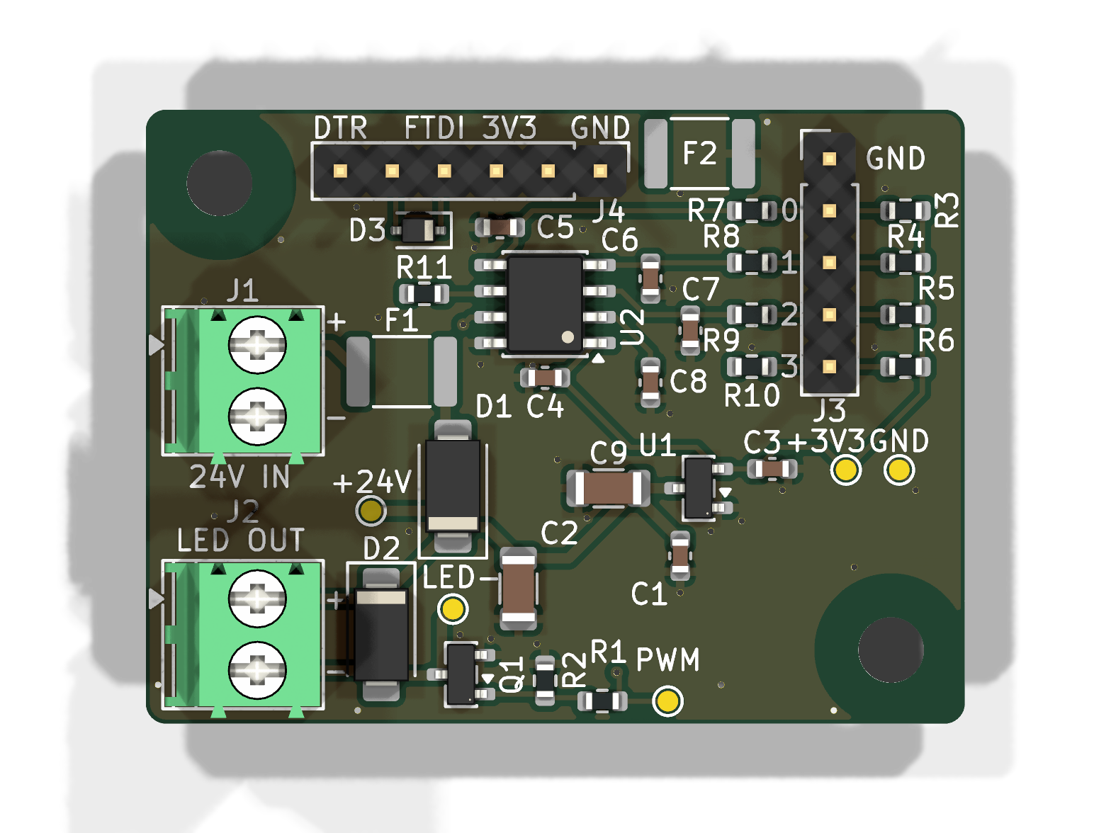
| Step | State |
|---|---|
| Schematic | Done. ERC: 0 violations. check_netlist.py: matches docs/netlist.txt |
| Placement | Done. Schematic parity clean |
| Routing | In progress. DRC: 0 violations; 5 unrouted connections (three HB_GND links to F2, UPDI_BUS R11–D3, SEL3 C8–R10). GND pours stitched with 32 vias |
| Parts | Every line has a manufacturer part carried by Mouser; see Parts |
| Firmware | Not started (spec section 9) |
| Path | Contents |
|---|---|
led-pwm-4bit.kicad_pro | Project: JLCPCB constraints, net classes (Default, Power) |
led-pwm-4bit.kicad_sch | Schematic, one sheet, KiCad standard symbols only |
led-pwm-4bit.kicad_pcb | Board |
led-pwm-4bit.kicad_dru | Custom DRC rules (JLCPCB limits, 0.5 mm power tracks) |
check_netlist.py | Compares the schematic netlist with docs/netlist.txt |
scripts/export-fab.sh | Runs ERC, netlist check and DRC, then writes fab/ |
fab/ | Schematic PDF, BOM, Mouser order CSV, position file, renders; Gerbers once DRC is clean |
All parts are chosen from manufacturers Mouser stocks, and each was checked against
its manufacturer's datasheet for package, pinout and ratings. Capacitor values were
also checked against DC-bias data.
fab/led-pwm-4bit-bom.csv is the full BOM and fab/led-pwm-4bit-mouser-order.csv
is in Mouser's BOM-tool format (BOARDS=n scripts/export-fab.sh scales it). The
order rounds the resistors, capacitors and D3 up to at least 10 with spares, which
costs less than the exact count at Mouser's single-piece prices.
The Mouser part-number column is left empty on purpose. Mouser blocks automated
access, so no Mouser number could be read off its live listing, and a guessed
number can import cleanly and still be the wrong part. Mouser's BOM tool matches
each line on the manufacturer part number instead. Once a Mouser number is
confirmed, add a field named Mouser to that symbol and the export carries it.
| Ref | Part | Notes |
|---|---|---|
| U1 | Microchip MCP1792T-3302H/CB | 55 V input LDO, SOT-23A |
| U2 | Microchip ATTINY412-SSN | Tube; ATtiny212-SSN also fits |
| Q1 | ROHM RTR030N05HZGTL | 45 V, RDS(on) ≤ 95 mΩ at VGS 2.5 V. The 60 V IRLML0060 is not rated below 4.5 V gate drive |
| D1, D2 | Diodes Inc B160-13-F | 60 V 1 A Schottky, SMA |
| D3 | onsemi BAT54HT1G | SOD-323, pin 1 cathode (BAT54J is out of stock at Mouser) |
| F1 | Littelfuse 1812L050/60MR | 0.5 A hold, 60 V, Imax 10 A |
| F2 | Bel Fuse 0ZCG0010FF2C | 0.1 A hold, 60 V, Imax 100 A; Hackerboard/programmer ground return |
| C1 | Murata GRM188R61H225KE11D | 2.2 µF 50 V X5R 0603, about 0.4 µF at 24 V |
| C2, C9 | Murata GRM31CR71H475MA12L | 4.7 µF 50 V X7R 1206, about 2.7 µF each at 24 V |
| C3 | Samsung CL10A106MP8NQWC | 10 µF 10 V X5R 0603, about 5.9 µF at 3.3 V |
| C4 | KEMET C0603C104K5RACTU | 100 nF 50 V X7R |
| C5–C8 | KEMET C0603C103K5RACTU | 10 nF 50 V X7R |
| R1–R11 | YAGEO RC0603FR-07…L | 1 % 0603; R3–R10 are all 10 kΩ |
| J1, J2 | Phoenix Contact 1984617 | PT 1,5/2-3,5-H, the part the footprint is drawn for |
| J3 | Würth 61300511121 | 1×5 2.54 mm header |
| J4 | Würth 61300611121 | 1×6 2.54 mm header |
No 10 µF 50 V X7R in 1206 was in stock at Mouser. The Murata 4.7 µF X7R keeps more capacitance at 24 V than any 10 µF 1206 part Mouser stocks.
+24V_IN, VIN_F, +24V, LED_NEG, GND) defaults to
0.5 mm, and DRC rejects anything narrower. Signals default to 0.25 mm.HB_GND joins J3 pin 1, J4 pins 1–2 and F2 pad 1. A 0.25 mm track is enough,
and it survives the brief fault current before F2 trips. J3.1 to J4.1 runs easily
on B.Cu. Keep it out of the GND pour: F2 is the only connection between the two
grounds.scripts/export-fab.sh refills the pours before its DRC, without saving the board.| Pin 1 | Pin 2 | Pin 3 | Pin 4 | Pin 5 | Pin 6 | |
|---|---|---|---|---|---|---|
| J1 24 V in | +24 V | GND | ||||
| J2 LED strip | Strip + | Strip − | ||||
| J3 Hackerboard J6 pins 1–5 | GND (via F2) | out0 | out1 | out2 | out3 | |
| J4 FTDI adapter | GND (via F2) | CTS (GND via F2) | VCC (n.c.) | TXD | RXD / UPDI | DTR (n.c.) |
Hackerboard J6 is a 1×10 2.54 mm footprint, usually bare holes. Its pin 1 is the
square pad by the GND label at the 0 end. A straight 1×5 cable from J6 pins 1–5
to J3 matches pin for pin.
J4 takes any USB-serial adapter in the standard FTDI pin order with 3.3 V logic (FT232R, CP2102, or a CH340 that really runs at 3.3 V). The SerialUPDI network (D3 and R11) is on the board, so the adapter needs no modification.
Power the board from 24 V. J4's VCC pin is not connected.
Plug the adapter in with its GND on J4 pin 1 (the GND end of the header).
Flash with avrdude 8.x:
avrdude -c serialupdi -p t412 -P /dev/cu.usbserial-XXXX -U flash:w:firmware.hex:ior pymcuprog:
pymcuprog write -t uart -u /dev/cu.usbserial-XXXX -d attiny412 -f firmware.hex --erase --verifyKeep the default 115200 baud at 3.3 V. In the Arduino IDE with megaTinyCore, pick "SerialUPDI - SLOW: 57600 baud", a 10 MHz clock and BOD 2.6 V. Never change the UPDI/reset pin fuse: recovery would then need a 12 V programmer.
A Microchip programmer (Atmel-ICE, MPLAB SNAP, PICkit) connects to J4 pin 5 (UPDI) and pin 1 (GND), with its target-voltage sense lead on TP2 (+3V3) and the board powered from 24 V. Leave "power target from tool" off.
M267 R3 B0    ; once: all expander pins are outputs (firmware default)
M267 R1 B15   ; level 15 (full on); B0 = off, B1..B14 in between
The level persists in the printer's EEPROM. While the printer boots, or when the cable is unplugged, the inputs float high and the strip is off.
python3 check_netlist.pyscripts/export-fab.shThe script runs ERC (--severity-all --exit-code-violations), the netlist check and
DRC with --schematic-parity after refilling the pours. It writes Gerbers and
separate plated and non-plated drill files only when DRC reports no violations and
no unrouted connections.
HB_GND) behind a 0.1 A PPTC,
and R7–R10 are 10 kΩ instead of 1 kΩ.| Qty | Value | Footprint | References |
|---|---|---|---|
| 8 | 10k | Resistor_SMD:R_0603_1608Metric | R3, R4, R5, R6, R7, R8, R9, R10 |
| 4 | 10n 50V X7R | Capacitor_SMD:C_0603_1608Metric | C5, C6, C7, C8 |
| 2 | 4.7u 50V X7R | Capacitor_SMD:C_1206_3216Metric | C2, C9 |
| 2 | B160 | Diode_SMD:D_SMA | D1, D2 |
| 2 | M3 | MountingHole:MountingHole_3.2mm_M3 | H1, H2 |
| 1 | +24V | TestPoint:TestPoint_Pad_D1.0mm | TP1 |
| 1 | +3V3 | TestPoint:TestPoint_Pad_D1.0mm | TP2 |
| 1 | 0.1A 60V | Fuse:Fuse_1812_4532Metric | F2 |
| 1 | 0.5A 60V | Fuse:Fuse_1812_4532Metric | F1 |
| 1 | 100 | Resistor_SMD:R_0603_1608Metric | R1 |
| 1 | 100k | Resistor_SMD:R_0603_1608Metric | R2 |
| 1 | 100n 50V X7R | Capacitor_SMD:C_0603_1608Metric | C4 |
| 1 | 10u 10V X5R | Capacitor_SMD:C_0603_1608Metric | C3 |
| 1 | 2.2u 50V X5R | Capacitor_SMD:C_0603_1608Metric | C1 |
| 1 | 24V IN | TerminalBlock_Phoenix:TerminalBlock_Phoenix_PT-1,5-2-3.5-H_1x02_P3.50mm_Horizontal | J1 |
| 1 | 470 | Resistor_SMD:R_0603_1608Metric | R11 |
| 1 | ATtiny412-SSN | Package_SO:SOIC-8_3.9x4.9mm_P1.27mm | U2 |
| 1 | BAT54HT1G | Diode_SMD:D_SOD-323 | D3 |
| 1 | FTDI-UPDI | Connector_PinHeader_2.54mm:PinHeader_1x06_P2.54mm_Vertical | J4 |
| 1 | GND | TestPoint:TestPoint_Pad_D1.0mm | TP3 |
| 1 | HACKERBOARD | Connector_PinHeader_2.54mm:PinHeader_1x05_P2.54mm_Vertical | J3 |
| 1 | LED STRIP | TerminalBlock_Phoenix:TerminalBlock_Phoenix_PT-1,5-2-3.5-H_1x02_P3.50mm_Horizontal | J2 |
| 1 | LED- | TestPoint:TestPoint_Pad_D1.0mm | TP5 |
| 1 | MCP1792T-3302H/CB | Package_TO_SOT_SMD:SOT-23 | U1 |
| 1 | PWM | TestPoint:TestPoint_Pad_D1.0mm | TP4 |
| 1 | RTR030N05HZG | Package_TO_SOT_SMD:SOT-23 | Q1 |
Meisterschulen-am-Ostbahnhof-Munchen/JC8012P4A1C_I_W_Y_CAN
JC8012P4A1C_I_W_Y addon PCB for CAN-Bus


iandchasse/silkscreen-pcb
Silkscreen: open-hardware ESP32-S3 e-paper reader mainboard (KiCad 9). Formerly the de-link hub.


EwoudVV/ducktop2
An open-source 16-inch laptop designed from scratch.


magnus188/aegir
Open-source ESP32-P4 trimix analyzer prototype for technical diving,

benkrasnow/1v2-boost-converter
Schematics and PCB layout for a boost converter 0.9V minimum input, 30A maximum input current
It measures 40 × 30 mm and has 2 copper layers, 1.6 mm thick.
39 parts, built around the ATTINY412-SSN, RC0603FR-0710KL, B160-13-F(MS) and 0ZCG0010FF2C. The full list of its parts is on this page, with links to each part's symbol and footprint where PCBKit's library has them.
From the hyiger/led-pwm-4bit repository on GitHub, at the commit this page was made from: the board is led-pwm-4bit.kicad_pcb and its schematic led-pwm-4bit.kicad_sch. PCBKit opens the board in the browser, with nothing to install.
Its repository states no licence, so its author keeps all rights: ask hyiger before reusing the design.