
2 layers68.8 × 53.6 mm
Relatively Universal ROM Programmer
AndersBNielsen/Relatively-Universal-ROM-Programmer
Hardware to program W27C512 EEPROM or any 24/28/32 pin ROM requiring from 5V to 27V programming voltage.
149 parts257GPL-3.0
 house4hack/PCBFactory1
Our PCB Factory to be ;)
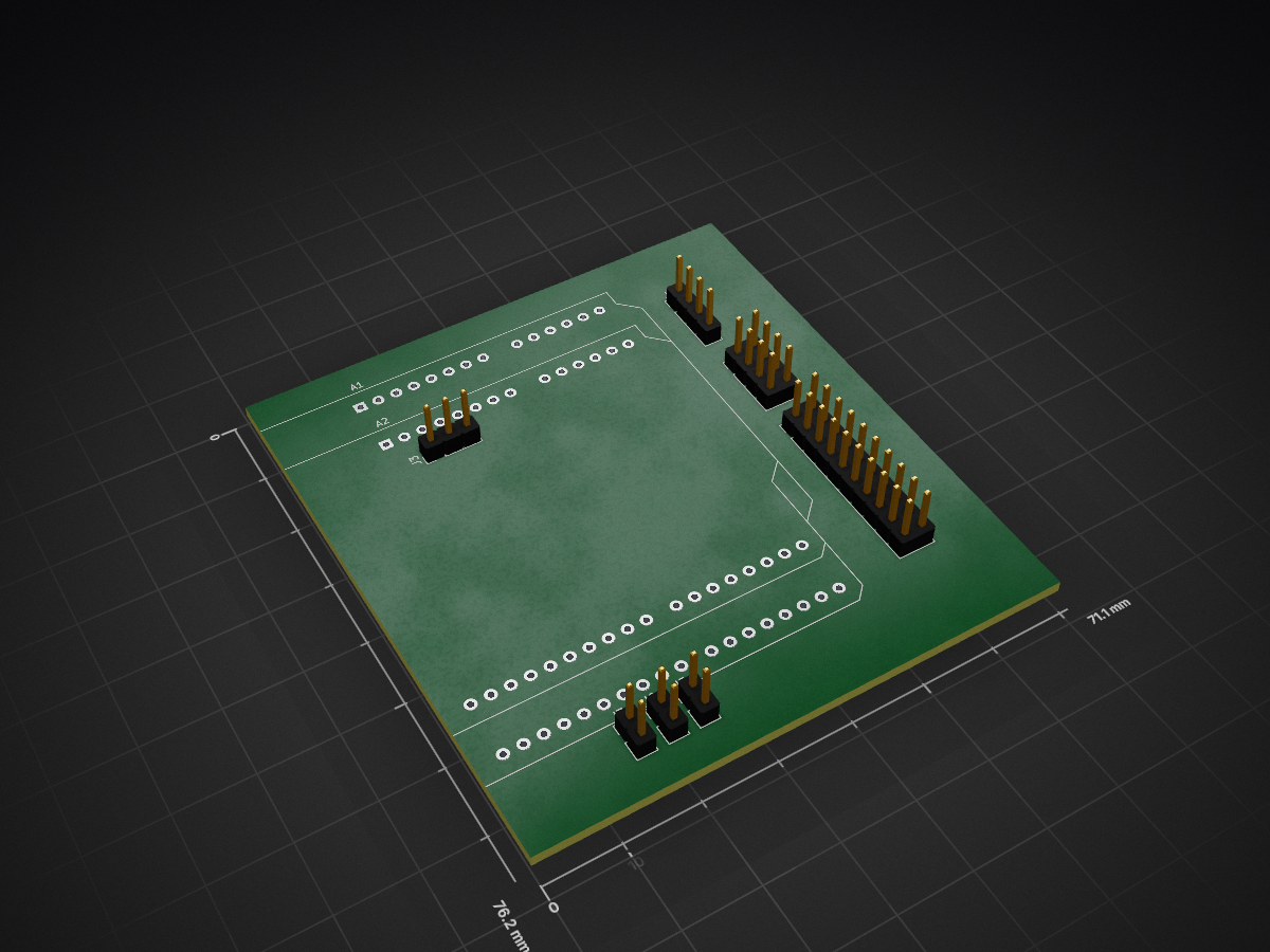
DaughterBrdInterface is an open-source printed circuit board by house4hack, from the house4hack/PCBFactory repository on GitHub, published under the MIT licence. It is a 2-layer board of 71.1 × 76.2 mm with 9 parts on 47 nets, routed with 142 tracks and 0 vias.
It is built around the ARDUINO UNO R3. It belongs with the AVR (ATmega, ATtiny) boards of this library.
A major impediment to be able to realise our projects quickly is the process to manufacture the PCBs required. Chinese companies like PCBWay and JLPCB provide exeptional service and low cost, but even with (for the industry) very short turn around times, this still means that projects are put on hold for a few weeks.
The danger of this delay is that it allows Squirrels 1 to manifest! To combat these Squirrels, we decided we needed a quick way to prototype PCBs, and the PCB Factory was born! Note, this project was the result of a squirrel, which just goes to show how insiduos these wretched beasts are!
in addition to the Squirrels, this project is also the offspring of other dubios parents.
The physical Hardware started its life as a 3d Printer called 3drag (https://reprap.org/wiki/3drag). It was donated to House4Hack and after not getting any love for a while, it was repurposed as the base for our PCB Factory.
The Controlling Software is the next evolution/remix of a stalled project that combined vision and CNC control to automate the drilling of etched PCBs.
Unlike the above, the CNC control software for the Hardware is based on the excellent GRBL project
We start with a blank PCB, which we coat with a protective layer of paint 2 or UV curable film. The PCBFactory will then burn away the protective layer around the tracks and leave a protective layer over the tracks so that when we etch the board, the protected areas are not etched away and only the unprotected areas are etched away. Furthermore it will be able to drill all the neccessary holes, and even mill the edges.
The relevant folders for these are linked below.
The Hardware is the skeleton and muscles of the factory. The 3drag donor printer is relativley unique in 3d printer hardware as the bed moves in the X & Y but is fixed in the z direction.
This makes this a great foundatiion for the PCB Factory as the tools will remain stationary while the work object is moved below.
The intent is to fix the gantry and allow each tool to move independently in the Z direction. To facilitate multiple tools, the tools themselves will be moved into the work position laterally on the gantry.
The custom fixtures needed i.e. z axis for spindles & laser, Gantry design etc is also located here.
The Firmware is the brain of the hardware, it receives commands from the software and directs the hardware how to act. Entirely based on GRBL, the firmware will be modified to allow the control of multiple tools.
The Software is the part of the process that acccepts the PCB Gerber files, and translates these into instructions (GCODE) that the firmware can understand.
'Squirrels' is the term used to describe the danger and temptation that newer, sexier projects become more attractive to the maker than the current project that has been delayed. As in "Look! A Sqirrel!" ↩
Paint must be Acrylic Spray Paint - See allow to dry completely before lasering. more coats == more lasing but better "potential" resistance to etching. Lasing paint leaves carbonised paint residue, this MUST be removed before etching. Possibe. ↩
| Qty | Value | Footprint | References |
|---|---|---|---|
| 1 | Arduino_UNO_R3 | Module:Arduino_UNO_R3 | A2 |
| 1 | Arduino_UNO_R3_CNC | Module:Arduino_UNO_R3 | A1 |
| 1 | Conn_01x04 | Connector_PinHeader_2.54mm:PinHeader_1x04_P2.54mm_Vertical | J4 |
| 1 | LCD POWER SELECT | Connector_PinHeader_2.54mm:PinHeader_1x03_P2.54mm_Vertical | J3 |
| 1 | LIMIT SWITCHES | Connector_PinHeader_2.54mm:PinHeader_2x04_P2.54mm_Vertical | J2 |
| 1 | PWM_TOOL1 | Connector_PinHeader_2.54mm:PinHeader_1x02_P2.54mm_Vertical | J5 |
| 1 | PWM_TOOL2 | Connector_PinHeader_2.54mm:PinHeader_1x02_P2.54mm_Vertical | J6 |
| 1 | PWM_TOOL3 | Connector_PinHeader_2.54mm:PinHeader_1x02_P2.54mm_Vertical | J7 |
| 1 | TO MASTER | Connector_PinHeader_2.54mm:PinHeader_2x10_P2.54mm_Vertical | J1 |
It measures 71.1 × 76.2 mm and has 2 copper layers, 1.6 mm thick.
9 parts, built around the ARDUINO UNO R3. The full list of its parts is on this page, with links to each part's symbol and footprint where PCBKit's library has them.
From the house4hack/PCBFactory repository on GitHub, at the commit this page was made from: the board is Electronics/PCB Factory/DaughterBrdInterface/DaughterBrdInterface.kicad_pcb. PCBKit opens the board in the browser, with nothing to install.
Its repository publishes it under the MIT licence: you may reuse it on that licence's terms (keep the author's notice, and for a copyleft licence share your changes alike).
AndersBNielsen/Relatively-Universal-ROM-Programmer
Hardware to program W27C512 EEPROM or any 24/28/32 pin ROM requiring from 5V to 27V programming voltage.

AlanFord/self-balancing-stick
Dual Axis Reaction Wheel Inverted Pendulum

Edging-Machines/Edging-Machines
This repository is intended to contain as much information as possible about building, designing, prototyping, and using automated edging machines.

PedroCNeves/AC_ChargingStation
A learning project to create an EV AC Charging station based on an Arduino Uno

jonsag/arduTester
An arduino component tester based on https://create.arduino.cc/projecthub/plouc68000/ardutester-v1-13-the-arduino-uno-transistor-tester-dbafb4


ICRS/101
The all-new open source Robotics 101 course from ICRS. It's specifically designed to be run in hackspaces, after school clubs and university societies.
