2 layers
Encoder
byrantech/laptop
anyon_e, a highly integrated, high end, open source laptop. Attempt the impossible.
7 parts4.3kMIT
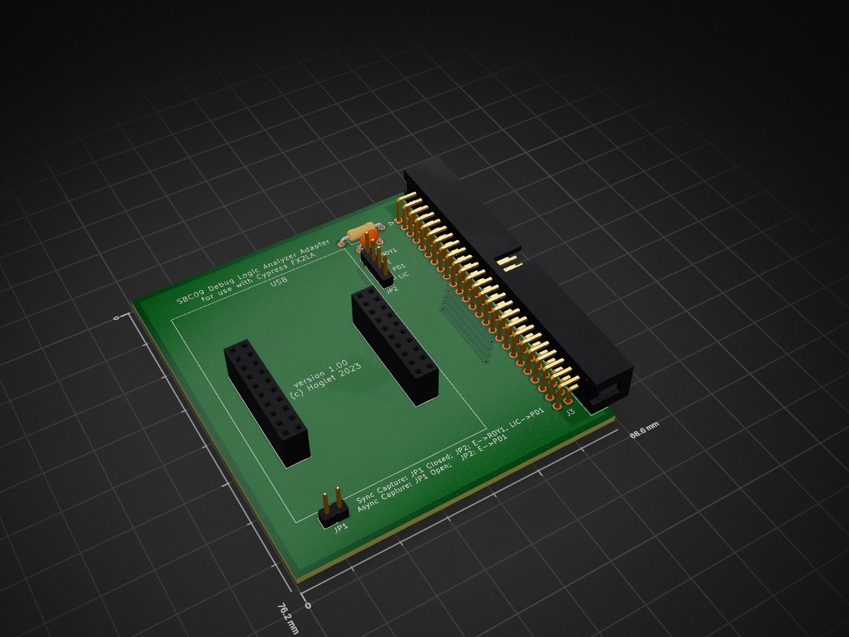
 hoglet67/sbc09_debugger1
6809 Decoder Logic Analyser Adapter PCB
Sbc09 debugger is an open-source printed circuit board by hoglet67, from the hoglet67/sbc09_debugger repository on GitHub. It is a 2-layer board of 68.6 × 76.2 mm with 7 parts on 67 nets, routed with 109 tracks and 8 vias.
Its parts include 3 connectors, 1 capacitor and 1 resistor. It belongs with the interfaces and adapters and sensors and measurement boards of this library.
| Qty | Value | Footprint | References |
|---|---|---|---|
| 2 | Conn_02x10_Odd_Even | Connector_PinSocket_2.54mm:PinSocket_2x10_P2.54mm_Vertical | J1, J2 |
| 1 | C_Small | Capacitor_THT:C_Disc_D4.7mm_W2.5mm_P5.00mm | C1 |
| 1 | Conn_01x04_Male | Connector_PinHeader_2.54mm:PinHeader_1x04_P2.54mm_Vertical | JP2 |
| 1 | Conn_02x25_Odd_Even | Connector_IDC:IDC-Header_2x25_P2.54mm_Horizontal | J3 |
| 1 | Jumper_2_Open | Connector_PinHeader_2.54mm:PinHeader_1x02_P2.54mm_Vertical | JP1 |
| 1 | R_Small | Resistor_THT:R_Axial_DIN0207_L6.3mm_D2.5mm_P10.16mm_Horizontal | R1 |
It measures 68.6 × 76.2 mm and has 2 copper layers, 1.6 mm thick.
7 parts. The full list of its parts is on this page, with links to each part's symbol and footprint where PCBKit's library has them.
From the hoglet67/sbc09_debugger repository on GitHub, at the commit this page was made from: the board is sbc09_debugger.kicad_pcb and its schematic sbc09_debugger.kicad_sch. PCBKit opens the board in the browser, with nothing to install.
Its repository states no licence, so its author keeps all rights: ask hoglet67 before reusing the design.
byrantech/laptop
anyon_e, a highly integrated, high end, open source laptop. Attempt the impossible.


AxxAxx/AxxSolder
STM32 Based soldering station for JBC cartridges, 9-24 VDC and USB-PD power


jamro/tiny-engineer
A small desktop robot that brings an AI coding assistant to life, physically acting out when it reads files, thinks, writes code, and finishes work.

hoglet67/RGBtoHDMI
Bare-metal Raspberry Pi project that provides pixel-perfect sampling of Retro Computer RGB/YUV video and conversion to HDMI
