2 layers51.9 × 25.9 mm

 HeyPCB/esp32-s3-devkit
ESP32-S3 dev board in the DevKitC-1 layout (31 x 64 mm, 4 layers, KiCad 10), built through HeyPCB's MCP server
Esp32-s3-devkit is an open-source printed circuit board by HeyPCB, from the HeyPCB/esp32-s3-devkit repository on GitHub, published under the MIT licence. It is a 4-layer board of 31 × 64 mm with 30 parts on 43 nets, routed with 397 tracks and 47 vias.
It is built around the ESP32-S3-WROOM-1-N8R8, AMS1117-3.3 and USBLC6-2SC6, with the WS2812B and 1N5819W among its other parts. Its parts include 12 capacitors, 6 resistors, 4 diodes, 3 ICs and 3 connectors. It belongs with the microcontroller boards boards and the ESP32 boards of this library.


A 31 × 64 mm ESP32-S3 development board laid out like Espressif's DevKitC-1: the WROOM-1 module at the top with its antenna on the edge, an 18-pin header down each side, three WS2812B LEDs, and USB-C between RST and BOOT.
An agent built it through HeyPCB's MCP server: blocks, parts, nets, hand placement, routing and checks, all as tool calls. KiCad 10 opens the files directly, and the board is on Circuit World to open or fork in HeyPCB (sign-in required).
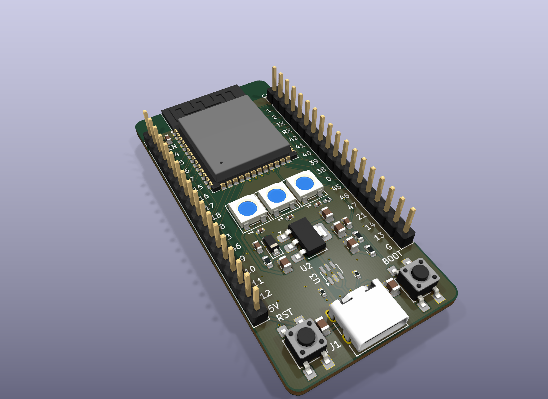
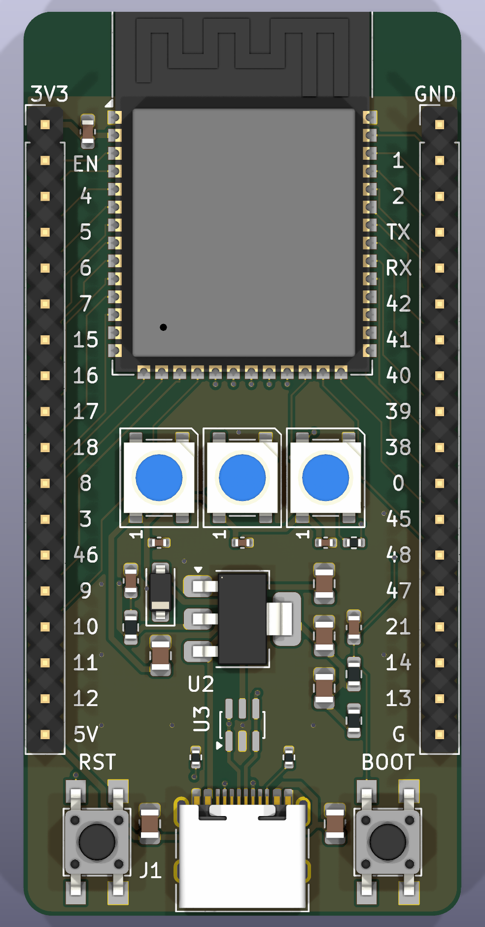
Every part has an LCSC number in the BOM.
Headers are 2.54 mm pitch, 27.94 mm (1.1 in) between rows. Pin 1 is at the antenna end on both sides.
| Pin | Left (J2) | Right (J3) |
|---|---|---|
| 1 | 3V3 | GND |
| 2 | EN (reset) | IO1 |
| 3 | IO4 | IO2 |
| 4 | IO5 | TXD0 |
| 5 | IO6 | RXD0 |
| 6 | IO7 | IO42 |
| 7 | IO15 | IO41 |
| 8 | IO16 | IO40 |
| 9 | IO17 | IO39 |
| 10 | IO18 | IO38 |
| 11 | IO8 | IO0 (BOOT) |
| 12 | IO3 | IO45 |
| 13 | IO46 | IO48 (LED data) |
| 14 | IO9 | IO47 |
| 15 | IO10 | IO21 |
| 16 | IO11 | IO14 |
| 17 | IO12 | IO13 |
| 18 | 5V (USB VBUS) | GND |
Measured on this revision:
| Check | Result |
|---|---|
| DRC, HeyPCB | 0 errors, 0 unconnected |
| DRC, KiCad 10.0.6 run locally | 0 errors, 0 unconnected |
| ERC | 0 errors |
| HeyPCB verify (DRC, ERC, artwork copper, electrical rules, simulation, IR drop, physical, DFM, placement, thermal) | all 10 pass |
| Fab readiness (JLCPCB) | ready to order, 14 checks passed |
Warnings the board still carries:
| Path | What it is |
|---|---|
esp32-s3-devkit.kicad_pro, .kicad_sch, .kicad_pcb | The KiCad 10 project |
heypcb-libs/ | The one footprint not in KiCad's standard library (USBLC6-2SC6, SOT-23-6), wired up by fp-lib-table |
design.json | The HeyPCB design the schematic and board are generated from |
fab/ | Gerbers and drill files, BOM and pick-and-place (CPL) for JLCPCB assembly |
images/ | KiCad 3D renders |
MIT. See LICENSE.
| Qty | Value | Footprint | References |
|---|---|---|---|
| 6 | 10uF | Capacitor_SMD:C_0805_2012Metric | C2, C3, C4, C5, C11, C12 |
| 3 | 100nF | Capacitor_SMD:C_0402_1005Metric | C8, C9, C10 |
| 3 | 100nF | Capacitor_SMD:C_0603_1608Metric | C1, C6, C7 |
| 3 | 10k | Resistor_SMD:R_0603_1608Metric | R1, R4, R5 |
| 3 | WS2812B | LED_SMD:LED_WS2812B_PLCC4_5.0x5.0mm_P3.2mm | D1, D2, D3 |
| 2 | 5.1k | Resistor_SMD:R_0402_1005Metric | R2, R3 |
| 1 | 1N5819W | Diode_SMD:D_SOD-123 | D4 |
| 1 | 330 | Resistor_SMD:R_0402_1005Metric | R6 |
| 1 | AMS1117-3.3 | Package_TO_SOT_SMD:SOT-223-3_TabPin2 | U2 |
| 1 | BOOT | Button_Switch_SMD:SW_SPST_TL3305A | SW1 |
| 1 | ESP32-S3-WROOM-1-N8R8 | RF_Module:ESP32-S3-WROOM-1 | U1 |
| 1 | Left | Connector_PinHeader_2.54mm:PinHeader_1x18_P2.54mm_Vertical | J2 |
| 1 | RST | Button_Switch_SMD:SW_SPST_TL3305A | SW2 |
| 1 | Right | Connector_PinHeader_2.54mm:PinHeader_1x18_P2.54mm_Vertical | J3 |
| 1 | USB-C | Connector_USB:USB_C_Receptacle_HRO_TYPE-C-31-M-12 | J1 |
| 1 | USBLC6-2SC6 | HeyPCB_Verified:SOT95P280X145-6N | U3 |
It measures 31 × 64 mm and has 4 copper layers, 1.6 mm thick.
30 parts, built around the ESP32-S3-WROOM-1-N8R8, AMS1117-3.3, USBLC6-2SC6 and WS2812B. The full list of its parts is on this page, with links to each part's symbol and footprint where PCBKit's library has them.
From the HeyPCB/esp32-s3-devkit repository on GitHub, at the commit this page was made from: the board is esp32-s3-devkit.kicad_pcb and its schematic esp32-s3-devkit.kicad_sch. PCBKit opens the board in the browser, with nothing to install.
Its repository publishes it under the MIT licence: you may reuse it on that licence's terms (keep the author's notice, and for a copyleft licence share your changes alike).

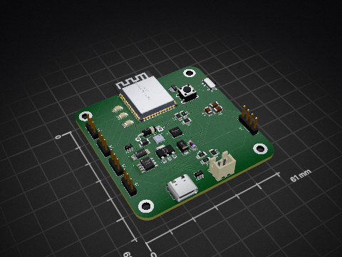

fubiniricci/NOVA-S3
A 40 × 30 mm, two-layer ESP32-S3 development board, designed and generated programmatically from the official KiCad libraries with a custom grid-based auto-router.

DylanLockyer/Black_Body
Electrical system for black body MKID tester


skrmsh/skirmish-hardware
Skirmish Hardware © 2022-2023 by Ole Lange is licensed under CC BY-NC-SA 4.0. To view a copy of this license, visit http://creativecommons.org/licenses/by-nc-sa/4.0/

shazmeenShz/ESP32-Flight-Controller
Custom 4-layer IoT-Ready ESP32 Flight Controller PCB designed in KiCad 8 featuring USB Type-C, CH340C, MP1584 power management, MPU6050 interface, and manufacturing-ready Gerber files.