Skip to the content
2 layers91.4 × 54.6 mmSine wave inverter, the printed circuit board in 3D

A collection of KiCad PCB designs developed during my Electronic Engineering degree (2024-28). Includes university projects, personal experiments, and custom components—featuring schematics, layouts, Gerber files, and documentation. Open-source hardware for education, collaboration, and real-world manufacturing.

Size
91.4 × 54.6 mm
Copper layers
2
Thickness
1.6 mm
Parts
41
Nets
26
Pads
105
Tracks, vias
202, 0
Pours
6
Routed
Yes
KiCad
KiCad 9.0 (file 20241229)
Created
5 Aug 2025
Updated
9 Nov 2025

Overview

Sine wave inverter is an open-source printed circuit board by hammadurrehman2006, from the hammadurrehman2006/kicad_lab repository on GitHub. It is a 2-layer board of 91.4 × 54.6 mm with 41 parts on 26 nets, routed with 202 tracks and 0 vias.

It is built around the FR207G, IRF3205 and S8050. Its parts include 12 resistors, 7 capacitors, 6 transistors, 5 connectors and 4 diodes. It belongs with the power boards of this library.

Main components

3

README

07_dc_boost_converter/README.md

Day 6 – Boost Converter (XL6009)

This is Day 6 of my 10-Day PCB Design Challenge. Today, I designed a Boost Converter circuit using the XL6009 regulator IC in KiCad.

A boost converter is a DC-DC step-up regulator that efficiently converts a lower input voltage into a higher output voltage, making it useful in power supply applications where the input source is lower than the required load voltage.


📜 Project Overview

This design uses the XL6009 boost regulator IC with supporting components to provide a stable adjustable output.

Key Components:

  • XL6009 Regulator IC (step-up DC-DC converter)

  • Inductor (33µH) for energy storage

  • Schottky diode (SS34) for rectification

  • Capacitors:

    • Input → 47µF/50V + 1µF
    • Output → 220µF/50V + 1µF
  • Potentiometer (RV1) to adjust output voltage

  • Resistor (R1) for feedback reference

  • Connectors for input & output terminals


🛠 Tools Used

  • KiCad → Schematic & PCB Design
  • GitHub → Version control & documentation

📂 Files in This Project

  • Schematic & PCB files (KiCad project)
  • Gerber files (for fabrication)
  • Drill files
  • Images (schematic, PCB layout, 3D preview)

📸 Project Images

Schematic
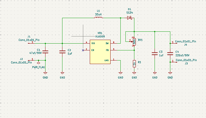
Schematic

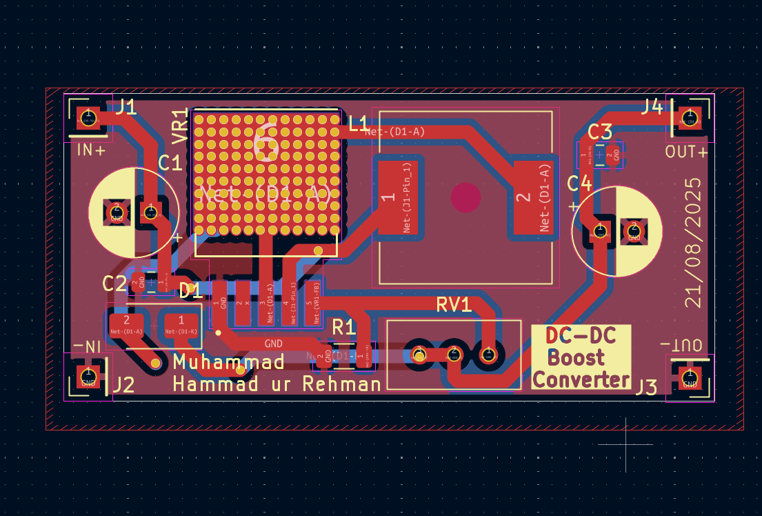
PCB Layout

Layout

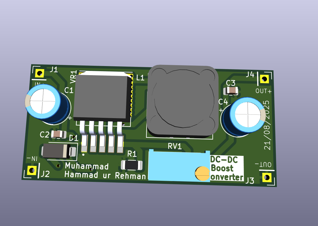
3D PCB Preview

3D PCB

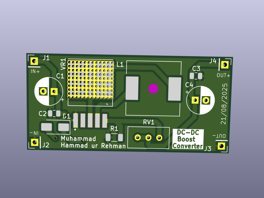
3D PCB Preview without Components

Board without components

📬 Repository Info

  • Folder Name: 07_dc_boost_converter
  • Author: Muhammad Hammad ur Rehman
  • License: Open for learning & educational purposes

⚡ With this boost converter, I can efficiently step up DC voltages — making it ideal for powering devices that require higher voltages from lower-voltage sources.


Parts

41
QtyValueFootprintReferences
410EResistor_THT:R_Axial_DIN0207_L6.3mm_D2.5mm_P7.62mm_HorizontalR3, R5, R9, R11
410KResistor_THT:R_Axial_DIN0207_L6.3mm_D2.5mm_P7.62mm_HorizontalR4, R6, R10, R12
4FR207GFR207G:DIOAD1300W80L670D310D1, D2, D3, D4
4IRF3205Package_TO_SOT_THT:TO-220-3_VerticalQ3, Q4, Q5, Q6
2100KResistor_THT:R_Axial_DIN0207_L6.3mm_D2.5mm_P7.62mm_HorizontalR7, R8
21KResistor_THT:R_Axial_DIN0207_L6.3mm_D2.5mm_P7.62mm_HorizontalR1, R2
21uFCapacitor_THT:CP_Radial_D5.0mm_P2.50mmC2, C4
1+BATTWA-MTAB:WA-MTAB_7471287MP1
1-BATTWA-MTAB:WA-MTAB_7471287MP2
10.1uCapacitor_THT:C_Disc_D4.3mm_W1.9mm_P5.00mmC3
10.1uFCapacitor_THT:C_Disc_D4.3mm_W1.9mm_P5.00mmC1
110KNXRT15WB333JA3A016:THERM_NXRT15WB333JA3A016RT1
110KPotentiometer_THT:Potentiometer_Bourns_3296W_VerticalRV1
110uCapacitor_THT:CP_Radial_D5.0mm_P2.50mmC7
12.2uFCapacitor_THT:C_Rect_L16.5mm_W6.0mm_P15.00mm_MKTC5
12200uFCapacitor_THT:CP_Radial_D12.5mm_P5.00mmC6
1AC/OUTTerminalBlock:TerminalBlock_bornier-2_P5.08mmJ5
1EGS002 MODULEConnector_PinSocket_2.54mm:PinSocket_1x17_P2.54mm_VerticalJ2
1FanB2B-XH-A__LF__SN_:JST_B2B-XH-A__LF__SN_J1
1LM7805_TO220Package_TO_SOT_THT:TO-220-3_VerticalU1
1LOGOLOGOG***
1NMOSPackage_TO_SOT_SMD:TO-252-2Q1
1S8050Package_TO_SOT_THT:TO-92_InlineQ2
1SwitchB2B-XH-A__LF__SN_:JST_B2B-XH-A__LF__SN_J3
1TR/INTerminalBlock:TerminalBlock_bornier-2_P5.08mmJ4

The 40 most common of 41 parts.

More from hammadurrehman2006/kicad_lab

6
  • 2 layers80.8 × 73.1 mm30A home automation using esp32, the printed circuit board in 3D

    30A home automation using esp32

    hammadurrehman2006/kicad_lab

    A collection of KiCad PCB designs developed during my Electronic Engineering degree (2024-28). Includes university projects, personal experiments, and custom components—featuring schematics, layouts, Gerber files, and…

    33 parts1
  • 2 layers55.4 × 40.6 mmTransformerless power supply, the printed circuit board in 3D

    Transformerless power supply

    hammadurrehman2006/kicad_lab

    A collection of KiCad PCB designs developed during my Electronic Engineering degree (2024-28). Includes university projects, personal experiments, and custom components—featuring schematics, layouts, Gerber files, and…

    19 parts1
  • 2 layers47.6 × 22.5 mmDc boost converter, the printed circuit board in 3D

    Dc boost converter

    hammadurrehman2006/kicad_lab

    A collection of KiCad PCB designs developed during my Electronic Engineering degree (2024-28). Includes university projects, personal experiments, and custom components—featuring schematics, layouts, Gerber files, and…

    13 parts1
  • 2 layers47.5 × 34 mmAc to dc converter, the printed circuit board in 3D

    Ac to dc converter

    hammadurrehman2006/kicad_lab

    A collection of KiCad PCB designs developed during my Electronic Engineering degree (2024-28). Includes university projects, personal experiments, and custom components—featuring schematics, layouts, Gerber files, and…

    11 parts1
  • 2 layers32.7 × 29.6 mmServo tester, the printed circuit board in 3D

    Servo tester

    hammadurrehman2006/kicad_lab

    A collection of KiCad PCB designs developed during my Electronic Engineering degree (2024-28). Includes university projects, personal experiments, and custom components—featuring schematics, layouts, Gerber files, and…

    10 parts1
  • 2 layers24 × 16.3 mmMotor driver, the printed circuit board in 3D

    Motor driver

    hammadurrehman2006/kicad_lab

    A collection of KiCad PCB designs developed during my Electronic Engineering degree (2024-28). Includes university projects, personal experiments, and custom components—featuring schematics, layouts, Gerber files, and…

    8 parts1

Similar boards

  • 2 layers90 × 44 mmDC AC Inverter EGS, the printed circuit board in 3D

    DC AC Inverter EGS

    stefaweb/DC-AC-Inverter-EGS

    Mini DC-AC Inverter with EGS002 module

    42 parts5
  • 2 layers92.6 × 52 mmSineWaveInverter, the printed circuit board in 3D

    SineWaveInverter

    ampnics/Project-10

    Mater KiCad with Projects is a series of lectures in which we are learning PCB designing

    44 parts2
  • 2 layers99.6 × 51.2 mm300w sine inverter kicad pcb, the printed circuit board in 3D

    300w sine inverter kicad pcb

    moksh-pcb-design/300W-SPWM-Pure-Sine-Wave-Inverter

    300W SPWM Pure Sine Wave Inverter PCB designed in KiCad 10 using EGS002 controller, IRF3205 MOSFET power stage, transformer interface, cooling fan control and manufacturing-ready outputs.

    39 parts1
  • 2 layers96.3 × 54.8 mmInverter, the printed circuit board in 3D

    Inverter

    ZawarAhmedKhan/SINEWAVE_INVERTER

    A robust 300W pure sine wave inverter PCB engineered around the EGS002 module, delivering clean, stable AC output with high efficiency.

    40 parts1
  • 2 layers102.7 × 51.2 mm300W SineWaveInverter EGS002, the printed circuit board in 3D

    300W SineWaveInverter EGS002

    midhun09-git/KiCad-PCB-Projects

    This repository contains a collection of my PCB design projects created using KiCad. Each project demonstrates a different type of power electronics or embedded circuit design.

    43 parts
  • 2 layers233.6 × 171.5 mmDIY Inverter Circuit - KiCAD, the printed circuit board in 3D

    DIY Inverter Circuit - KiCAD

    BaselMohamed802/EyeTalk

    An Accessible AAC Device Using Visual Speech to empower and help disabled people talk and communicate, as a graduation project for my

    172 parts1GPL-3.0
  • 4 layers153.7 × 108.5 mmVolPak-1000, the printed circuit board in 3D

    VolPak-1000

    raybello/KICAD-PCBs

    Repository for KICAD PCB Designs

    189 parts
  • 2 layers77.7 × 73.2 mmBMT BionX Minimum Translator vereinfacht, the printed circuit board in 3D

    BMT BionX Minimum Translator vereinfacht

    stancecoke/BionX_Minimal_Translator

    Drive your BionX motor with a no-name battery and a Kunteng LCD-display without any further BionX-components

    40 parts22GPL-3.0

Questions

How big is the Sine wave inverter PCB?

It measures 91.4 × 54.6 mm and has 2 copper layers, 1.6 mm thick.

What parts does the Sine wave inverter use?

41 parts, built around the FR207G, IRF3205 and S8050. The full list of its parts is on this page, with links to each part's symbol and footprint where PCBKit's library has them.

Where can I download the Sine wave inverter KiCad files?

From the hammadurrehman2006/kicad_lab repository on GitHub, at the commit this page was made from: the board is 11_sine_wave_inverter/sine_wave_inverter.kicad_pcb and its schematic 01_sp02_monitor/sp02_monitor.kicad_sch. PCBKit opens the board in the browser, with nothing to install.

Can I use the Sine wave inverter design in my own project?

Its repository states no licence, so its author keeps all rights: ask hammadurrehman2006 before reusing the design.