
2 layers60 × 100 mm

 hackclub/thing4
Many Hack Clubbers will add a tool or something to the same PCB consecutively, and at the end I'll get \10 made and send them off to some people you may or may not have seen on YouTube...
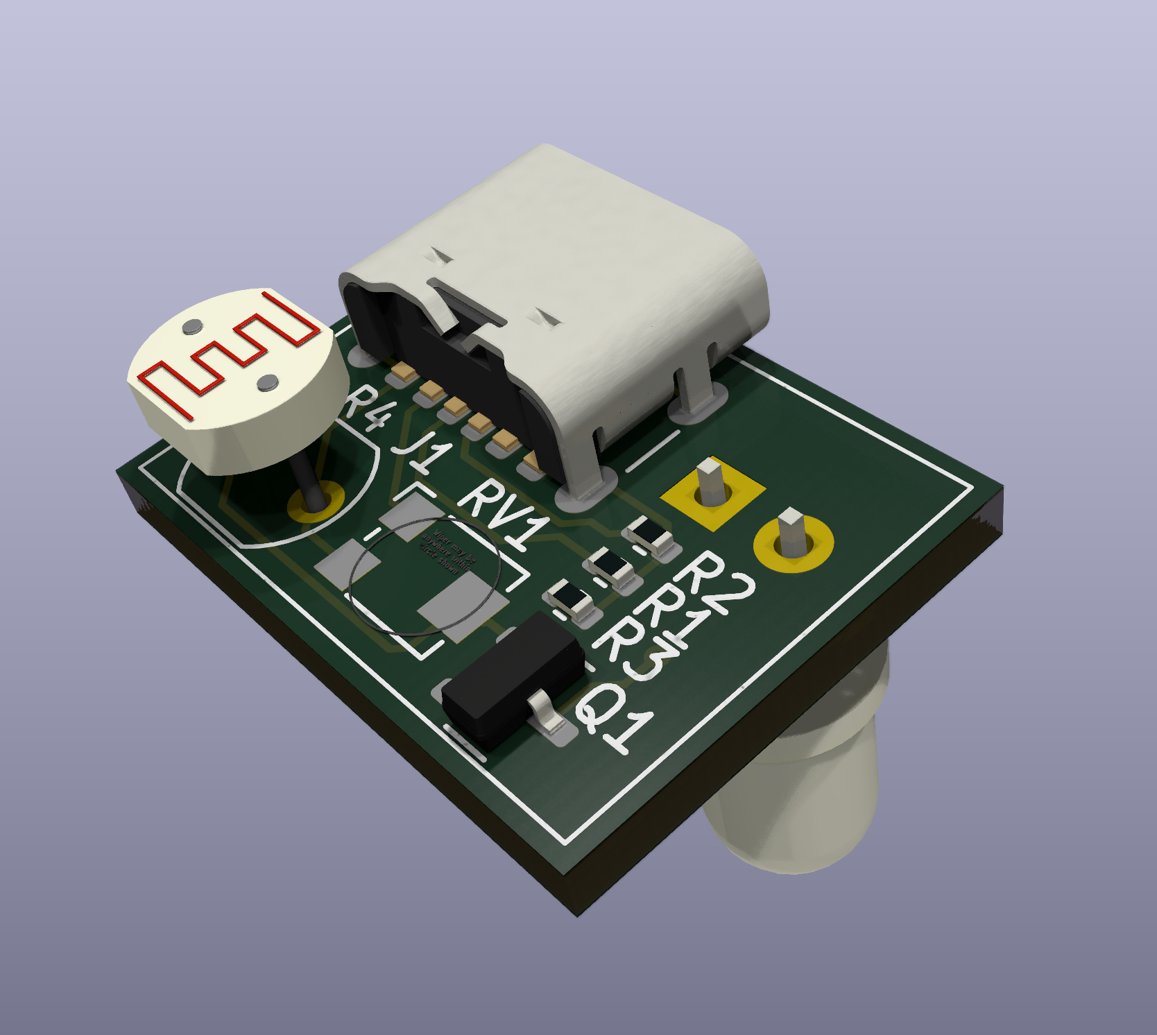
PCB2 is an open-source printed circuit board by hackclub, from the hackclub/thing repository on GitHub. It is a 2-layer board of 18 × 13.5 mm with 8 parts on 7 nets, routed with 59 tracks and 2 vias.
It is built around the T2N7002AK,LM. Its parts include 4 resistors, 1 diode, 1 transistor and 1 connector.

Hey! Welcome to The Thing!
Have you seen those 80-part Swiss Army knives? I want us to make a PCB with that level of esotericism; a sprawling, over-the-top monstrosity.
Many Hack Clubbers will add a tool or something to the same PCB consecutively, and at the end I'll get ~10 made and send them off to some people you may or may not have seen on YouTube... (and if you find me at a hackathon and you've added a subsystem to the board you may end up with one too (prob limited to 1 or 2)).
It'll end when 100 subsystems have been added or nobody adds a component for a week. Happy hacking!
/docs directory, add a folder titled IDX-USERNAME, where IDX is your number in line, and USERNAME is your GitHub username.
0-malted.doc.md: Your writeup. Include detail about your subsystem! How you designed it, your calculations, tests, everything. Don't use an LLM, make it interesting, tell me a story!! :Dpcb.png: A screenshot of the PCB in Kicad's PCB editor, showing the entire PCB.pcb-3d.png: Switch to View > 3D viewer and select "Render current view using raytracing". Again, we want to see the whole board!schematic.png: A screenshot of the whole board's schematic.cad.png (OPTIONAL): If someone designs an enclosure or something (wink wink nudge nudge), show me a screenshot of it. You only need to do this if you've changed it.bom.csv: Your bill of materials. Create and edit this manually. The price should be that of a single part (regardless of your quantity, on the line item for 100 pieces. It should be in USD without a dollar symbol.
/docs/0-malted/bom.csv. There's a template at /docs/bom-template.csv.9.0.x. Apparently, our project will be corrupted if we're on differing versions.Finding parts can be tricky. Here's how I found the USB-C receptable I used in my circuit;
| Qty | Value | Footprint | References |
|---|---|---|---|
| 2 | 5k1Ω | Resistor_SMD:R_0402_1005Metric | R1, R2 |
| 1 | 100kΩ | Potentiometer_SMD:Potentiometer_Bourns_TC33X_Vertical | RV1 |
| 1 | 150Ω | Resistor_SMD:R_0402_1005Metric | R3 |
| 1 | 3k-70kΩ | OptoDevice:R_LDR_5.1x4.3mm_P3.4mm_Vertical | R4 |
| 1 | LED | LED_THT:LED_D5.0mm_Clear | D1 |
| 1 | T2N7002AK | Package_TO_SOT_SMD:SOT-23 | Q1 |
| 1 | USB_C_Receptacle_PowerOnly_6P | Connector_USB:USB_C_Receptacle_GCT_USB4125-xx-x-0190_6P_TopMnt_Horizontal | J1 |
It measures 18 × 13.5 mm and has 2 copper layers, 1.6 mm thick.
8 parts, built around the T2N7002AK,LM. The full list of its parts is on this page, with links to each part's symbol and footprint where PCBKit's library has them.
From the hackclub/thing repository on GitHub, at the commit this page was made from: the board is PCB/PCB2.kicad_pcb and its schematic PCB/PCB2.kicad_sch. PCBKit opens the board in the browser, with nothing to install.
Its repository states no licence, so its author keeps all rights: ask hackclub before reusing the design.


introlab/t-top
T-Top is a tabletop robot designed with advanced audio and vision sensors, deep learning perceptual processing and telecommunication capabilities to provide richer interaction modalities and develop higher cognitive…


A-Neal/dmx-led-bar-v1
An FPGA-based 6-channel DMX decoder and LED fixture.
