
2 layers158.8 × 120.6 mm

 gnahiak2/getou_1
( This needs manual review cuz fallout project )
Getou is an open-source printed circuit board by gnahiak2, from the gnahiak2/getou_ repository on GitHub, published under the MIT licence. It is a 2-layer board of 60 × 116 mm with 25 parts on 26 nets, routed with 126 tracks and 9 vias.
It is built around the MX1A-11NN. Its parts include 12 diodes, 12 switches and 1 IC. It belongs with the RP2040 boards of this library.
Its pretty much a hackpad but i made it myself
Here's the Zine!
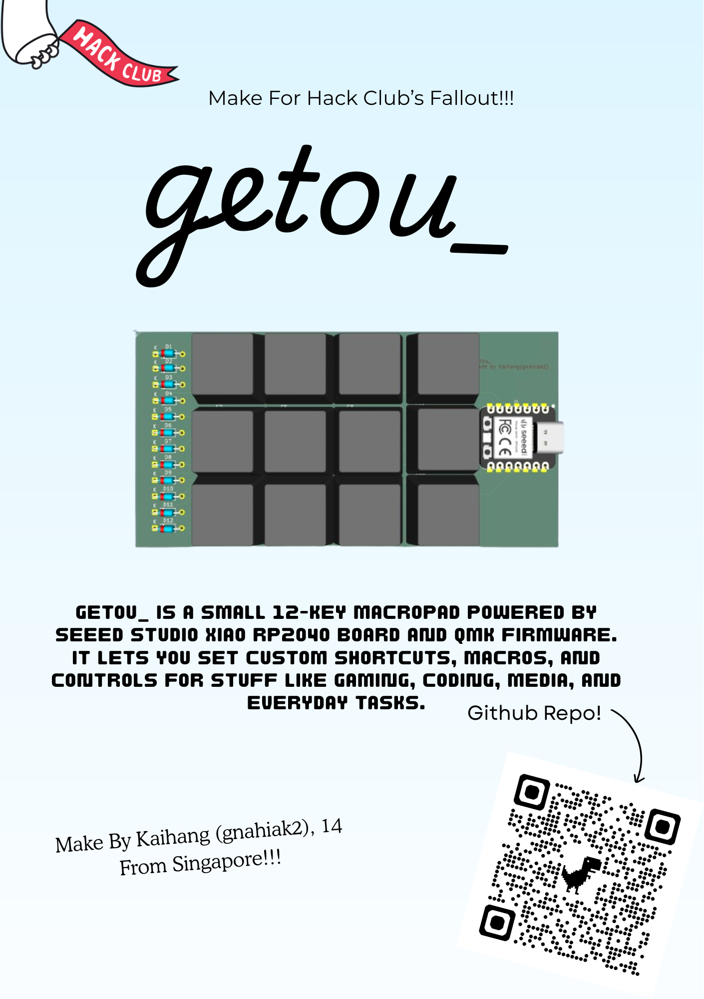
( This needs manual review cuz fallout project )
Firmware was made in C via qmk, the accompanying app was made in swift with the help of chatgpt
git clone https://github.com/gnahiak2/getou_.git
cd getou_qmk compile -kb getou_ -km defaultPlug in your USB-C Cable while holding the Boot button (marked B)
Drag the .uf2 file into the RP2040 and you're done!
AI was used for QMK
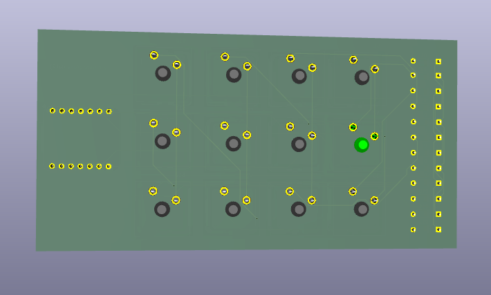
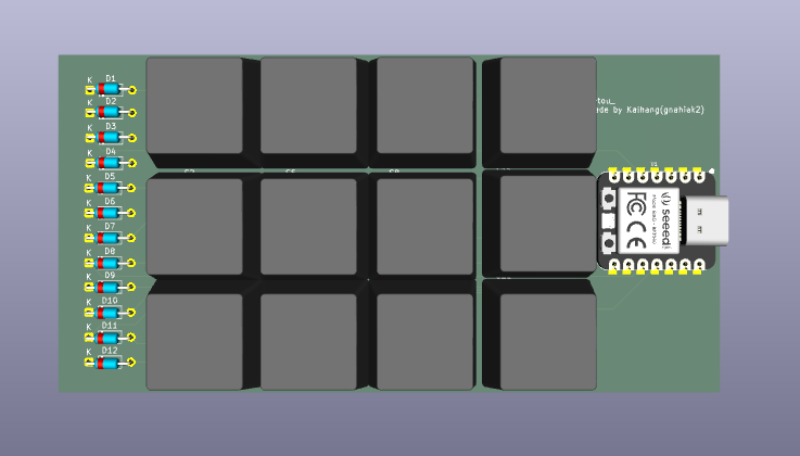
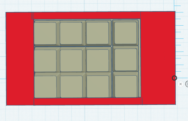
| Qty | Value | Footprint | References |
|---|---|---|---|
| 12 | 1N4148 | Diode_THT:D_DO-35_SOD27_P7.62mm_Horizontal | D1, D2, D3, D4, D5, D6, D7, D8, D9, D10, D11, D12 |
| 12 | MX1A-11NN | footprints:SW_MX1A-11NN | S1, S2, S3, S4, S5, S6, S7, S8, S9, S10, S11, S12 |
| 1 | XIAO-RP2040-DIP | footprints:XIAO-RP2040-DIP | U1 |
It measures 60 × 116 mm and has 2 copper layers, 1.6 mm thick.
25 parts, built around the MX1A-11NN. The full list of its parts is on this page, with links to each part's symbol and footprint where PCBKit's library has them.
From the gnahiak2/getou_ repository on GitHub, at the commit this page was made from: the board is KiCAD/GETOU_.kicad_pcb and its schematic KiCAD/GETOU_.kicad_sch. PCBKit opens the board in the browser, with nothing to install.
Its repository publishes it under the MIT licence: you may reuse it on that licence's terms (keep the author's notice, and for a copyleft licence share your changes alike).


axooexe/Macropad-s-PCB
This repository contains the schematics and PCB layout files for a custom 8switches and an encoder macropad.


