2 layers24.6 × 8.1 mm

 glovepost/atoplace2
KiCAD EDA automatic component placement tool
Layouts is an open-source printed circuit board by glovepost, from the glovepost/atoplace repository on GitHub, published under the MIT licence. It is a 2-layer board of 42 × 27 mm with 66 parts on 74 nets, routed with 488 tracks and 81 vias.
Its parts include 27 capacitors, 21 resistors, 5 diodes, 4 ICs and 2 switches.
 [blocked]



The AI Pair Designer for Professional PCB Layout
atoplace is an intelligent orchestration layer for PCB design that bridges the gap between schematic and physical layout. It automates the tedious 80% of design—placement optimization and DFM validation—while strictly adhering to "Manhattan" aesthetics and Signal Integrity (SI) best practices.
Designed to work seamlessly with atopile and KiCad.
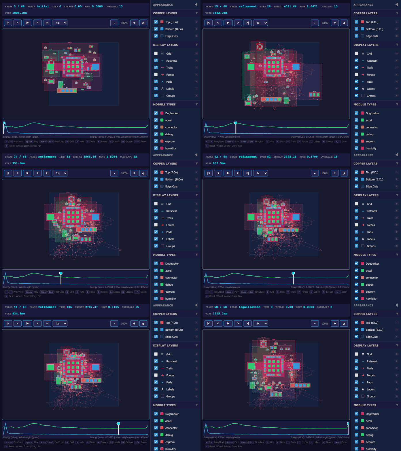
PCB layout automation has historically been "black box" and "messy"—producing organic, unreadable layouts that professional engineers reject. atoplace takes a different approach:
.kicad_pcb file. You can take over manually at any second.atopile projects with ato-lock.yaml parsing, module-aware grouping, and atoplace.lock sidecar persistence to preserve placements across rebuilds.pip install atoplacepcbnew Python API)Pro Tip: atoplace works best when run using the Python interpreter bundled with KiCad:
macOS:
/Applications/KiCad/KiCad.app/Contents/Frameworks/Python.framework/Versions/Current/bin/python3 -m pip install atoplaceWindows:
"C:\Program Files\KiCad\8.0\bin\python.exe" -m pip install atoplaceAutomatically place components with "Manhattan" legalization:
atoplace place board.kicad_pcb --grid 0.5 --constraints "USB on left edge"Route all nets using the internal A* geometric planner:
atoplace route board.kicad_pcb --visualizeCheck your board against DFM rules (JLCPCB, OSH Park, etc.):
atoplace validate board.kicad_pcb --dfm jlcpcb_standardRefine your design using natural language:
atoplace interactive board.kicad_pcb
# > "Rotate U1 45 degrees"
# > "Move C1 closer to U1"
# > "Save"Expose atoplace tools to AI agents via the Model Context Protocol:
atoplace mcp --launchSee MCP Server section below for details.
ato-lock.yaml and module hierarchy integration.atoplace.lock Sidecar Persistence for atopile projects.atoplace/
├── board/ # Board abstraction & KiCad/Atopile adapters
│ ├── abstraction.py # Board, Component, Net, Pad data models
│ ├── kicad_adapter.py # KiCad pcbnew integration
│ ├── lock_file.py # atoplace.lock sidecar persistence
│ └── atopile_adapter.py # Atopile project loader
├── placement/ # Force-directed physics & Manhattan Legalizer
│ ├── force_directed.py # Physics Engine (Star Model, adaptive damping)
│ ├── legalizer.py # Manhattan Pipeline with PCA alignment
│ ├── module_detector.py # Functional module hierarchy analysis
│ ├── constraints.py # Placement constraints (Proximity, Edge, Zone, etc.)
│ └── visualizer.py # SVG delta visualization with frame capture
├── routing/ # A* Geometric Router
│ ├── astar_router.py # Core A* with Greedy Multiplier (w=2-3)
│ ├── manager.py # Multi-phase routing pipeline
│ ├── spatial_index.py # O(~1) collision detection via spatial hashing
│ ├── obstacle_map.py # Obstacle generation from board
│ ├── diff_pairs.py # Differential pair detection
│ ├── visualizer.py # Routing visualization with A* debug
│ └── fanout/ # BGA/QFN escape routing
├── visualization/ # Unified visualization system
│ └── assets/ # External JS/CSS for HTML viewer
│ ├── svg-delta-viewer.js # Interactive SVG playback engine
│ └── styles.css # KiCad-inspired dark themeatoplace includes a Model Context Protocol (MCP) server that exposes 40+ PCB design tools to LLM agents like Claude. This enables conversational PCB layout design with support for placement, routing, fanout generation, and design validation.
Just run:
python -m atoplace.mcp.launcherThat's it! The launcher:
Add to your MCP config:
{
  "mcpServers": {
    "atoplace": {
      "command": "python",
      "args": ["-m", "atoplace.mcp.launcher"]
    }
  }
}Note: Replace
pythonwith the path to your atoplace virtualenv Python if needed.
New! With KiCad 9+, atoplace can manipulate components in real-time without save/reload cycles. Changes appear instantly in your KiCad viewport!
Requirements:
kicad-python package: pip install kicad-pythonSetup:
# Install the kipy optional dependency
pip install atoplace[kipy]

# Or install directly
pip install kicad-python
Usage:
.kicad_pcb in KiCad 9+ PCB EditorATOPLACE_BACKEND=kipy python -m atoplace.mcp.launcherHow it works: The kipy backend connects directly to KiCad's IPC socket and uses the official API to update component positions in real-time. Native undo/redo (Cmd/Ctrl+Z) works seamlessly.
flowchart LR
    subgraph MCP["MCP Server (Python 3.10+)"]
        direction TB
        FastMCP[FastMCP]
        Tools[26 Layout Tools]
        Context[Context Generators]
    end

    subgraph KiPy["KiPy Backend (KiCad 9+)"]
        direction TB
        IPC[KiCad IPC API]
        LiveEdit[Real-time Updates]
        NativeUndo[Native Undo/Redo]
    end

    subgraph Bridge["KiCad Bridge (KiCad 8.x)"]
        direction TB
        pcbnew[pcbnew API]
        BoardIO[Board I/O]
        UndoRedo[Undo/Redo]
    end

    MCP <-->|"KiCad IPC\nSocket"| KiPy
    MCP <-->|"Unix Socket\nJSON-RPC"| Bridge
Backend Modes:
| Mode | KiCad Version | Real-time | How it works | Status |
|---|---|---|---|---|
kipy | 9.0+ | ✅ Yes | Direct IPC API connection | Default |
ipc | 8.0+ | ❌ No | File-based bridge process | Fallback |
direct | 8.0+ | ❌ No | Direct file manipulation | Fallback |
Note: KIPY mode is the primary backend for bleeding-edge development. It provides instant visual feedback in KiCad's viewport and native undo/redo integration. The server automatically falls back to IPC or direct mode if KIPY is unavailable.
| Category | Tools |
|---|---|
| Board Management | load_board, save_board, undo, redo |
| Placement Actions | move_absolute, move_relative, rotate, place_next_to, align_components, distribute_evenly, stack_components, arrange_pattern, cluster_around, lock_components |
| Discovery | find_components, get_board_summary, get_unplaced_components |
| Routing | route_board, route_net, detect_diff_pairs, get_routing_preview, analyze_pin_swaps, optimize_pin_swaps, export_pin_constraints |
| BGA/Fanout | detect_bga_components, fanout_component, fanout_all_bgas, get_fanout_preview |
| Context | inspect_region, get_semantic_grid, get_module_map |
| Validation | check_overlaps, validate_placement, run_drc, get_crossing_analysis |
| Optimization | optimize_placement, detect_modules, parse_constraint, get_atopile_context |
| Variable | Description | Default |
|---|---|---|
ATOPLACE_BACKEND | Backend mode: kipy, ipc, or direct | kipy (with fallback) |
ATOPLACE_USE_KIPY | Enable kipy mode (1 or true) | Deprecated - use ATOPLACE_BACKEND |
KICAD_PYTHON | Override KiCad Python path | Auto-detected |
ATOPLACE_LOG | Log file location | /tmp/atoplace.log |
Default behavior: The server attempts KIPY first, then falls back to IPC, then direct mode. For bleeding-edge KiCad 9+ users, no configuration is needed - KIPY mode activates automatically when KiCad is running with IPC enabled.
User: Load the board at examples/dogtracker/layouts/default/default.kicad_pcb

Claude: [Calls load_board tool]
Board loaded successfully:
- 37 components
- 72 nets

User: Find all the capacitors and align them horizontally

Claude: [Calls find_components with query="C", filter_by="ref"]
Found 12 capacitors: C1, C2, C3...

[Calls align_components with refs=["C1","C2",...], axis="y"]
Aligned 12 capacitors along the Y axis.

User: Check if there are any overlaps

Claude: [Calls check_overlaps]
No overlapping components detected. The placement is valid.

User: Save the board

Claude: [Calls save_board]
Board saved to: examples/dogtracker/layouts/default/default.placed.kicad_pcbWhen working with atopile projects, placement positions can be lost when ato build regenerates the KiCad board. The atoplace.lock sidecar file solves this by persisting component positions between builds.
After placement, atoplace automatically saves positions to a lock file next to the board:
my-project/
├── elec/
│   └── layout/
│       └── default/
│           ├── default.kicad_pcb
│           └── default.atoplace.lock  ← Saved positions
└── ato.yamlversion: 1
created: 2026-01-14T10:30:00
build: default
components:
U1:
x: 125.5
y: 80.0
rotation: 0.0
locked: true # User-approved position
module: mcu
C1:
x: 130.0
y: 85.5
locked: false # Auto-placed, can be re-optimized| Flag | Description |
|---|---|
--use-lock | Apply saved positions before placement |
--only-locked | Only restore locked: true positions |
--save-lock/--no-save-lock | Auto-save after placement (default: on) |
--lock-all | Mark all positions as user-approved |
# First placement - automatically saves lock file
atoplace place my-project/ --use-ato-modules

# After `ato build` regenerates board - restore positions
atoplace place my-project/ --use-lock

# Only restore approved positions, re-optimize others
atoplace place my-project/ --use-lock --only-locked

# Approve all current positions
atoplace place my-project/ --lock-allThe lock file uses Lock > Physics priority:
locked: true positions always preserved (user-approved)locked: false positions used as initial hints, can be re-optimizedMIT License - see LICENSE for details.
| Qty | Value | Footprint | References |
|---|---|---|---|
| 12 | 10kΩ ±1% 62.5mW | UNI_ROYAL_0402WGF1002TCE:R0402 | R4, R6, R7, R8, R9, R11, R12, R16, R18, R19, R20, R21 |
| 10 | 1µF ±10% 50V X5R | Samsung_Electro_Mechanics_CL10A105KB8NNNC:C0603 | C2, C5, C6, C7, C8, C9, C10, C11, C12, C13 |
| 4 | 100nF ±10% 16V X7R | Samsung_Electro_Mechanics_CL05B104KO5NNNC:C0402 | C14, C15, C17, C24 |
| 4 | 22µF ±20% 6.3V X5R | Samsung_Electro_Mechanics_CL21A226MQQNNNE:C0805 | C20, C21, C22, C23 |
| 3 | TWGMC_MBR0530:SOD-123_L2.7-W1.6-LS3.7-RD-1 | D1, D2, D3 | |
| 3 | 1µF ±10% 25V X5R | Samsung_Electro_Mechanics_CL05A105KA5NQNC:C0402 | C18, C25, C27 |
| 2 | ALPSALPINE_SKRPACE010:KEY-SMD_4P-L4.2-W3.2-P2.20-LS4.6 | SW1, SW2 | |
| 2 | 10µF ±10% 25V X5R | Samsung_Electro_Mechanics_CL21A106KAYNNNE:C0805 | C3, C4 |
| 2 | 4.7kΩ ±1% 62.5mW | UNI_ROYAL_0402WGF4701TCE:R0402 | R13, R14 |
| 1 | atopile_Logo_4x4mm:atopile_Logo_4x4mm | LOGO1 | |
| 1 | Hubei_KENTO_Elec_Blue_light_0603:LED0603-RD | LED1 | |
| 1 | BQ25185DLHR_BQ25185DLHR:WSON-10_L2.2-W2.0-P0.40-BL-EP_TI_DLH0010A | U4 | |
| 1 | TECH_PUBLIC_SI1308EDL:SOT-323-3_L2.0-W1.3-P1.30-LS2.1-BR | Q1 | |
| 1 | MOLEX_532610271:CONN-SMD_532610271 | U1 | |
| 1 | EEMB_BATTERY_LP402535:EEMB_BATTERY_LP402535 | B1 | |
| 1 | kinghelm_KH_TYPE_C_16P:USB-C-SMD_KH-TYPE-C-16P | USB1 | |
| 1 | Hubei_KENTO_Elec_KT_0603R:LED0603-RD | LED2 | |
| 1 | Espressif_Systems_ESP32_C3_MINI_1_N4:WIFIM-SMD_ESP32-C3-MINI-1 | U2 | |
| 1 | XUNPU_FPC_05F_24PH20:FPC-SMD_24P-P0.50_FPC-05F-24PH20 | FPC1 | |
| 1 | Texas_Instruments_TPS63020DSJR:VSON-14_L4.0-W3.0-P0.50-BL-EP_TI_DSJ | U3 | |
| 1 | 1.2MΩ ±1% 62.5mW | FOJAN_FRC0402F1204TS:R0402 | R2 |
| 1 | 10µF ±20% 6.3V X5R | Murata_Electronics_GRM155R60J106ME44D:C0402 | C26 |
| 1 | 18kΩ ±1% 62.5mW | YAGEO_RC0402FR_0718KL:R0402 | R17 |
| 1 | 1MΩ ±1% 62.5mW | UNI_ROYAL_0402WGF1004TCE:R0402 | R5 |
| 1 | 1µH ±20% 4.7A 18mΩ | cjiang_FNR4030S1R0MT:IND-SMD_L4.0-W4.0_FNR40XXS | L1 |
| 1 | 200kΩ ±1% 62.5mW | UNI_ROYAL_0402WGF2003TCE:R0402 | R1 |
| 1 | 22µF ±20% 6.3V X5R | Samsung_Electro_Mechanics_CL10A226MQ8NRNC:C0603 | C16 |
| 1 | 2kΩ ±1% 62.5mW | UNI_ROYAL_0402WGF2001TCE:R0402 | R15 |
| 1 | 3.3Ω ±1% 62.5mW | UNI_ROYAL_0402WGF330KTCE:R0402 | R3 |
| 1 | 4.7µF ±10% 16V X5R | Samsung_Electro_Mechanics_CL10A475KO8NNNC:C0603 | C19 |
| 1 | 4.7µF ±20% 10V X5R | Samsung_Electro_Mechanics_CL05A475MP5NRNC:C0402 | C1 |
| 1 | 470mΩ ±1% | YAGEO_RL0402FR_070R47L:R0402 | R10 |
| 1 | 68µH ±20% 50mA 6Ω | Taiyo_Yuden_LB2012T680M:L0805 | L2 |
It measures 42 × 27 mm and has 2 copper layers, 1.6 mm thick.
66 parts. The full list of its parts is on this page, with links to each part's symbol and footprint where PCBKit's library has them.
From the glovepost/atoplace repository on GitHub, at the commit this page was made from: the board is examples/hivehaus/src/products/espaper/layouts/default/default.kicad_pcb. PCBKit opens the board in the browser, with nothing to install.
Its repository publishes it under the MIT licence: you may reuse it on that licence's terms (keep the author's notice, and for a copyleft licence share your changes alike).


hackclub/OnBoard
💡 Join 1,000 teenagers and make your first PCB with a $100 grant!


famichu/MagLev_Switch_MX
The 3D printable magnetic levitation contactless switch with the linear output hall effect sensor.

mmccoyd/hillside
Family of split ergonomic keyboards with three rows of six or five keys and a generous thumb arc


Ardumower/ardumower
Develop an open source robotic lawn mower (HW+SW reference platform)