A small board for hat Rev 4 in the Huey head Rev 5 (Head/Rev5/Hat). It carries an ALPS RKJXM1015004 8-direction stick switch with a centre push, and screws to four bosses printed on the back of the lower panel.
HeliSR Rev4.0 is an open-source printed circuit board by genbean, from the genbean/UH1-Collective repository on GitHub, published under the GPL-3.0 licence. It is a 2-layer board of 39.3 × 33.6 mm with 33 parts on 34 nets, routed with 661 tracks and 78 vias.
It is built around the PCA9546AD, 74HC165D and TL1015AF160QG. Its parts include 11 resistors, 8 connectors, 4 capacitors, 3 ICs and 1 switch.
SearchHat Rev 1.0: breakout board for the SEARCH CONT hat
A small board for hat Rev 4 in the Huey head Rev 5 (Head/Rev5/Hat). It carries an ALPS RKJXM1015004 8-direction stick switch with a centre push, and screws to four bosses printed on the back of the lower panel. The switch's body comes through the panel's 13.5 mm hole and the cap goes on its stick.
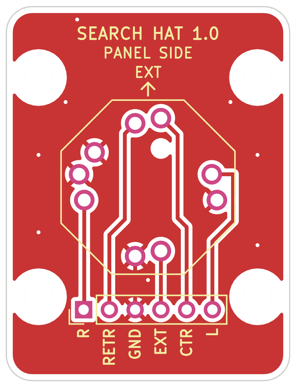
Front: faces the panel
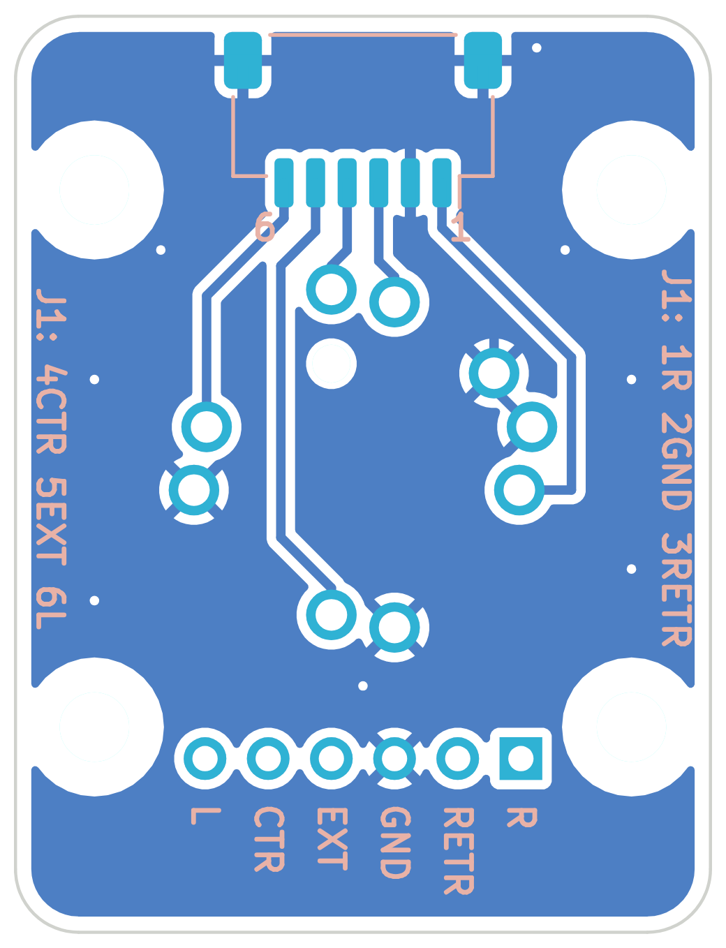
Back, mirrored: as you see it from behind
Size
22 × 29 mm, 2 layers, 1.6 mm FR4, 2 mm corners
Holes
Four 2.2 mm holes for M2 × 8 countersunk screws, 8.5 mm from the switch's centre each way (17 mm apart). Every track and both ground pours stop 2.2 mm from each hole's centre, clear of the 3.8 mm screw head
Switch
SW1, on the front, centred 11 mm from each long side and 14 mm below the top edge
Connector
J1, a 6-pin JST SH 1.0 mm side-entry header (SM06B-SRSS-TB), on the back at the top. The plug goes in from the top edge and the cable leaves upward
Wire pads
J2, six 2 mm-pitch plated holes (0.8 mm) along the bottom, to solder wires to instead of J1
Ground
Pours on both sides, joined by eight vias
The switch
The RKJXM1015004 has nine pins on two circles (9.9 and 10.7 mm) and a 1.1 mm locating peg. The footprint (SearchHat.pretty/SW_ALPS_RKJXM1015004) takes its pin centres from JLCPCB/EasyEDA's footprint for the part (LCSC C97432), which match the ALPS catalog's mounting-hole drawing: 1.0 mm holes for the pins, here with 1.6 mm pads, and a 1.2 mm unplated hole for the peg.
How it's wired inside, from the catalog's circuit diagram:
PUSH (three pins, joined inside) is the common of the four directions. Tilting the stick joins PUSH to A, B, C or D; a diagonal joins two neighbours, so it's an 8-way switch.
The centre push joins COM to PUSH.
GND is the metal frame.
So the board ties PUSH and GND to ground. A–D are the four directions and COM is the centre push. Seen from the front (as you look at the panel), and going by the catalog's lever drawing: A is up (EXT), C down (RETR), B left (L) and D right (R). The silkscreen on the front has an arrow marked EXT pointing up.
Pinout
Signal
Switch pin
J1 pin
J2 pad
HeliSR J2 pin
HeliSR input
R (right)
D
1
1
5
IN12
GND
PUSH ×3, GND
2 (and the mounting tabs)
3
1 or 10
RETR (down)
C
3
2
3
IN10
CTR (centre push)
COM
4
5
8
IN15 (spare; leave it off if you don't want a centre button)
EXT (up)
A
5
4
2
IN9
L (left)
B
6
6
4
IN11
These are the inputs the tact-switch hats used (IN9–IN12 as EXT, RETR, L, R), so the existing profiles work as they are. The centre push is new. IN15 is spare, so bind it in a profile if you want it.
The pin order isn't GND first. On J1 the signals follow the order their switch pins come round the ring, so every track on the back runs without a crossing; on J2 the same goes for the front. The silkscreen names them:
J1: "1" and "6" mark its ends on the back. Up the long edges, "J1: 1R 2GND 3RETR" and "J1: 4CTR 5EXT 6L". Seen from behind, pin 1 is on the right.
J2: each pad's name is under it, on both sides.
The lead: cut a 6-pin JST SH jumper (A06SR06SR30K152A) in half, as for the HeliSR's ports. Plug one end into J1 and splice its wires into the HeliSR's J2 loom as in the table. Check pin 1 with a meter: cut jumpers come in both "same side" and "reversed" versions. Or leave J1 off and solder five or six wires to J2.
Building it
J1 first, on the back, while the board is flat. Line its pins up on the pads, then tack and solder the two mounting tabs.
SW1 on the front: its peg goes in the 1.2 mm hole, so it only fits one way. Hold it flat against the board and solder its nine pins on the back. It must sit flat: it is what places the stick in the panel's hole.
Check with a meter, with nothing pressed: no direction or CTR is joined to GND. Tilt each way and press the middle: each joins its own signal to GND, and each diagonal joins two.
DRC:kicad-cli pcb drc reports no violations and nothing unconnected. The rules are the HeliSR boards' cheap-fab rules: 0.127 mm minimum track and clearance, with this board's net class at 0.3 mm tracks and 0.2 mm clearance. Two exceptions are written into SearchHat_Rev1.0.kicad_dru, each limited to the parts it names:
The lower M2 holes' library courtyards overlap J2's by about 0.5 mm. The screw head itself is 0.9 mm from the nearest pad.
The left PUSH pin gets one thermal spoke on the back, where R runs past it. A ground track on the back and the front pour join it as well.
Fit in the head:Head/Rev5/check_r5.py places the board, the switch, J1 and a plug with its wires against the body, the toggles and the HeliSR board: all clear. The tightest spot is the end of J1's plug, 2.2 mm below the lower box's top wall. From about 12 mm behind the panel the slot up to the upper box is open, so the wires turn straight back and go up to the HeliSR.
Not checked
Nothing is ordered or built yet. Still to check on a real part:
the footprint, against the switch itself: the pin centres come from two sources that agree, but neither is ALPS's own PCB drawing;
that A is really up, as the catalog's lever drawing reads. If a direction comes out wrong, swap its inputs in the profile, or swap the wires;
whether a countersunk M2 head sits well on the board's plain 2.2 mm hole. A small washer under each head is fine if it doesn't.
Gerbers with Protel extensions and a job file, plus the PTH and NPTH drill files: send it to any PCB maker
SearchHat_Rev1.0_Top.png, _Bottom_mirrored.png
The pictures above
SearchHat_Rev1.0_mech.json
The outline, holes and parts' places, measured from the switch's centre. Head/Rev5/Hat/hat4_r5.py reads it, so the panel's bosses always match the board
tools/gen_searchhat.py
Builds the board from scratch: parts, hand-placed tracks, pours, silkscreen, rules and the JSON
tools/export_searchhat.py
Writes the Gerbers and the pictures (the HeliSR's export script, sized for this board)
A small board for hat Rev 4 in the Huey head Rev 5 (Head/Rev5/Hat). It carries an ALPS RKJXM1015004 8-direction stick switch with a centre push, and screws to four bosses printed on the back of the lower panel.
A small board for hat Rev 4 in the Huey head Rev 5 (Head/Rev5/Hat). It carries an ALPS RKJXM1015004 8-direction stick switch with a centre push, and screws to four bosses printed on the back of the lower panel.
Universal Ingenic SoC development platform: one carrier + per-SoC interposer modules (T10 through A1, any package) on a DDR4 card edge, with an ESP32-S3 BMC for autonomous LLM-driven development.
123 parts1GPL-3.0
Questions
How big is the HeliSR Rev4.0 PCB?
It measures 39.3 × 33.6 mm and has 2 copper layers, 1.6 mm thick.
What parts does the HeliSR Rev4.0 use?
33 parts, built around the PCA9546AD, 74HC165D and TL1015AF160QG. The full list of its parts is on this page, with links to each part's symbol and footprint where PCBKit's library has them.
Where can I download the HeliSR Rev4.0 KiCad files?
From the genbean/UH1-Collective repository on GitHub, at the commit this page was made from: the board is PCB/HeliSR_Rev4.0/HeliSR_Rev4.0.kicad_pcb. PCBKit opens the board in the browser, with nothing to install.
Can I use the HeliSR Rev4.0 design in my own project?
Its repository publishes it under the GPL-3.0 licence: you may reuse it on that licence's terms (keep the author's notice, and for a copyleft licence share your changes alike).