
2 layers57.3 × 19 mm

 GadgetReboot/S_NES_Controller_Breakout1
Breakout board to decode NES or SNES controller buttons as separate GPIO outputs from ATTiny26
GR SNES Breakout is an open-source printed circuit board by GadgetReboot, from the GadgetReboot/S_NES_Controller_Breakout repository on GitHub. It is a 2-layer board of 45.7 × 51.7 mm with 26 parts on 33 nets, routed with 251 tracks and 33 vias.
It is built around the ATTINY26L-8PU. Its parts include 16 resistors, 4 capacitors, 4 connectors and 1 IC. It belongs with the retro computing and games and interfaces and adapters boards and the AVR (ATmega, ATtiny) boards of this library.
Breakout board to decode NES or SNES controller buttons as separate GPIO outputs from ATTiny26
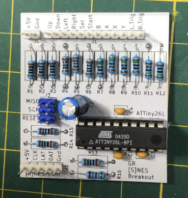
| Qty | Value | Footprint | References |
|---|---|---|---|
| 15 | 100r | Resistor_THT:R_Axial_DIN0309_L9.0mm_D3.2mm_P12.70mm_Horizontal | R1, R2, R3, R4, R5, R6, R7, R8, R9, R10, R11, R12, R13, R14, R15 |
| 3 | 100nF | Capacitor_THT:C_Disc_D3.8mm_W2.6mm_P2.50mm | C1, C3, C4 |
| 1 | 10K | Resistor_THT:R_Axial_DIN0309_L9.0mm_D3.2mm_P12.70mm_Horizontal | R16 |
| 1 | 10uF 16v | Capacitor_THT:CP_Radial_D5.0mm_P2.50mm | C2 |
| 1 | ATtiny26L-8PU | Package_DIP:DIP-20_W7.62mm | U1 |
| 1 | Conn_01x02 | Connector_PinHeader_2.54mm:PinHeader_1x02_P2.54mm_Vertical | J4 |
| 1 | Conn_01x05 | Connector_PinHeader_2.54mm:PinHeader_1x05_P2.54mm_Vertical | J2 |
| 1 | Conn_01x12 | Connector_PinHeader_2.54mm:PinHeader_1x12_P2.54mm_Vertical | J1 |
| 1 | Conn_02x03_Odd_Even | Connector_PinHeader_2.54mm:PinHeader_2x03_P2.54mm_Vertical | J3 |
| 1 | LOGO | _Custom_Footprints:pcb way logo | G*** |

hackclub/OnBoard
💡 Join 1,000 teenagers and make your first PCB with a $100 grant!


harbaum/galagino
A Galaga, Pac-Man and Donkey Kong arcade emulator for the ESP32

Luos-io/luos_engine
Open-source and real-time orchestrator for cyber-physical-systems, to easily design, test and deploy embedded applications and digital twins.

google/walt
A device for measuring latency of physical sensors and outputs on phones and computers

It measures 45.7 × 51.7 mm and has 2 copper layers, 1.6 mm thick.
26 parts, built around the ATTINY26L-8PU. The full list of its parts is on this page, with links to each part's symbol and footprint where PCBKit's library has them.
From the GadgetReboot/S_NES_Controller_Breakout repository on GitHub, at the commit this page was made from: the board is KiCad/GR_SNES_Breakout.kicad_pcb. PCBKit opens the board in the browser, with nothing to install.
Its repository states no licence, so its author keeps all rights: ask GadgetReboot before reusing the design.