
2 layers148 × 84.5 mm
Panel daisy
ohmtech-rdi/eurorack-blocks
Software to Hardware Prototyping for Eurorack using C++, Max/Gen~ or Faust
259 parts410

 GadgetReboot/FET_Matching3
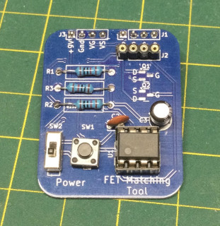
N Channel JFET Matching PCB
FET Matching is an open-source printed circuit board by GadgetReboot, from the GadgetReboot/FET_Matching repository on GitHub. It is a 2-layer board of 33.1 × 41.4 mm with 14 parts on 7 nets, routed with 103 tracks and 10 vias.
It is built around the TL072. Its parts include 3 resistors, 3 connectors, 2 capacitors, 2 transistors and 2 switches.
N Channel JFET Matching PCB
Used with a multimeter to read VGS on a JFET so that it acts like a 10K resistor.
eg. Some JFETs may look like a 10K resistor when VGS = -1.5v
while others look like a 10K resistor when VGS = -0.350v
FETs can be measured and sorted in groups with similar VGS specs when needed.
| Qty | Value | Footprint | References |
|---|---|---|---|
| 3 | 10K | Resistor_THT:R_Axial_DIN0309_L9.0mm_D3.2mm_P12.70mm_Horizontal | R1, R2, R3 |
| 3 | Conn_01x04 | Connector_PinHeader_2.54mm:PinHeader_1x04_P2.54mm_Vertical | J1, J2, J3 |
| 1 | 100nF | Capacitor_THT:C_Disc_D3.4mm_W2.1mm_P2.50mm | C2 |
| 1 | 10uF | Capacitor_THT:CP_Radial_D5.0mm_P2.50mm | C3 |
| 1 | BF545C | Package_TO_SOT_SMD:SOT-23 | Q2 |
| 1 | BSR56 | Package_TO_SOT_SMD:SOT-23 | Q1 |
| 1 | LOGO | _Custom_Footprints:pcb way logo | G*** |
| 1 | SW_Push | Footprints:PushButton | SW1 |
| 1 | SW_SPST | Button_Switch_THT:SW_Slide-03_Wuerth-WS-SLTV_10x2.5x6.4_P2.54mm | SW2 |
| 1 | TL072 | Package_DIP:DIP-8_W7.62mm | U1 |
ohmtech-rdi/eurorack-blocks
Software to Hardware Prototyping for Eurorack using C++, Max/Gen~ or Faust

ctag-fh-kiel/ctag-tbd
CTAG TBD >>to be determined<< an extendible open source Eurorack sound module

plinkysynth/plinky_public
a public release of the plinky sw and hw


matthewcieplak/super-sixteen
Code and schematics for the Super Sixteen Eurorack sequencer

mzuelch/CATs-Eurosynth
Analog Synth Eurorack Modules

StoneRose35/cortexguitarfx
guitar effects processor implemented on various arm cortex platforms
It measures 33.1 × 41.4 mm and has 2 copper layers, 1.6 mm thick.
14 parts, built around the TL072. The full list of its parts is on this page, with links to each part's symbol and footprint where PCBKit's library has them.
From the GadgetReboot/FET_Matching repository on GitHub, at the commit this page was made from: the board is KiCad/FET_Matching.kicad_pcb and its schematic KiCad/FET_Matching.kicad_sch. PCBKit opens the board in the browser, with nothing to install.
Its repository states no licence, so its author keeps all rights: ask GadgetReboot before reusing the design.