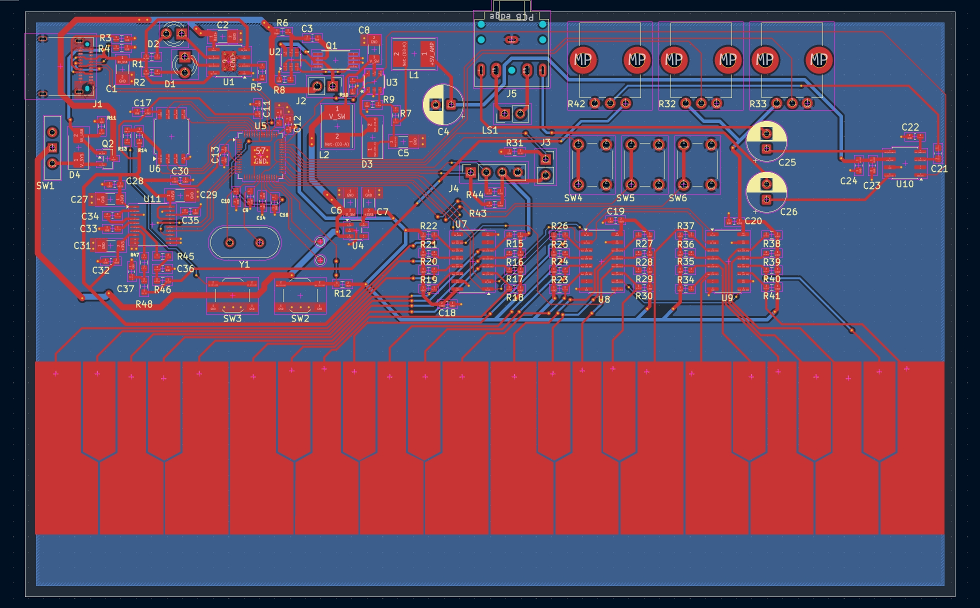
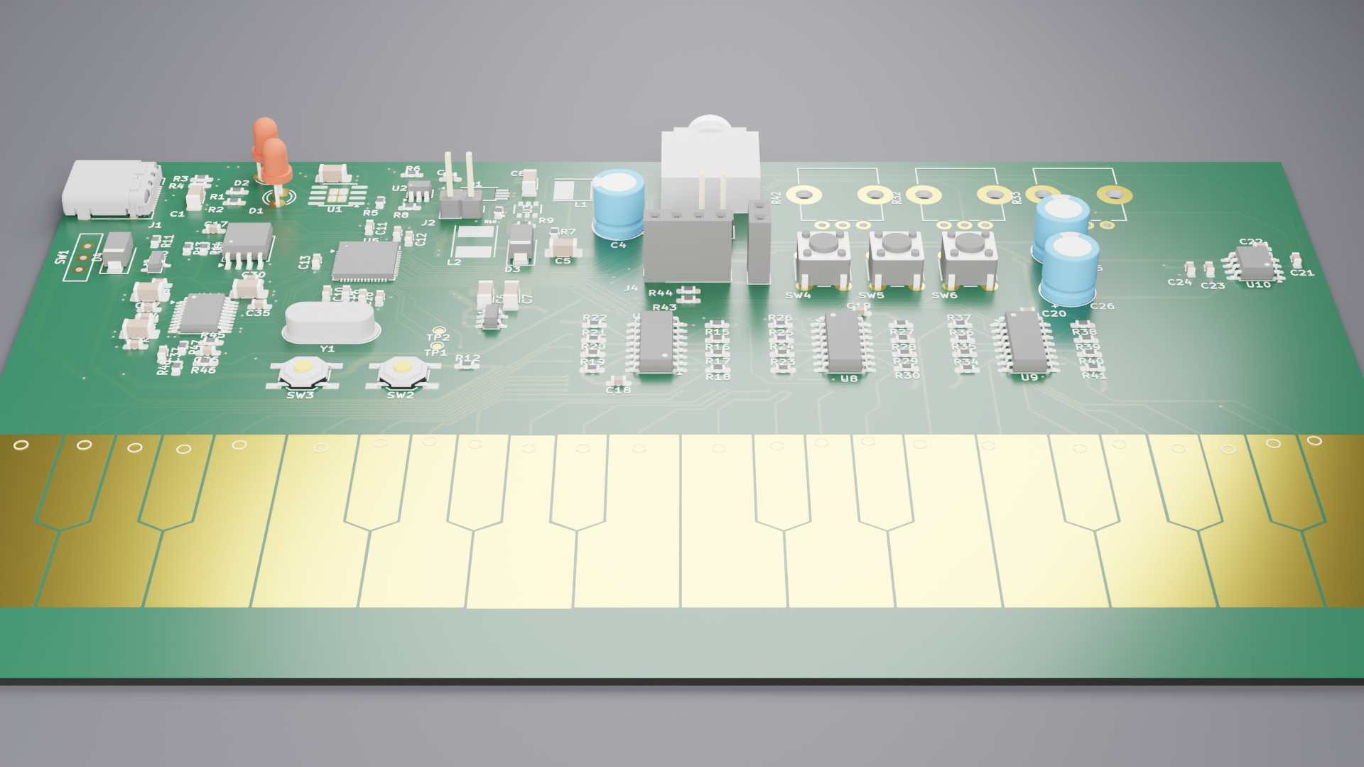
Deneme is an open-source printed circuit board by g210101021, from the g210101021/OpenStylophone-RP2040 repository on GitHub. It is a 2-layer board of 151 × 95 mm with 143 parts on 123 nets, routed with 1,142 tracks and 187 vias.
It is built around the RP2040, PAM8302AADCR and TPFP6291LR-G1, with the W25Q32JVSSIQ, 74HC165D and AP2112K-3.3 among its other parts. Its parts include 48 resistors, 37 capacitors, 11 ICs, 6 switches and 5 connectors. It belongs with the RP2040 boards of this library.
A Modern Open-Source Hardware Reimagining of the Iconic 1968 Stylophone Synthesizer. Powered by Raspberry Pi RP2040 Dual-Core Silicon, High-Fidelity 32-Bit I2S DAC, Integrated Battery Management, and a 24-Key Touch Keyboard Matrix.
The OpenStylophone-RP2040 is a standalone, open-source electronic musical instrument designed in KiCad. It pays homage to the legendary 1968 stylus-operated pocket synth while elevating every analog and digital subsystem to modern embedded audio engineering standards on a compact 2-layer printed circuit board ($151.0,\text{mm} \times 95.0,\text{mm}$).
Traditional stylophones relied on simplistic analog 555-timer / oscillator resistor-ladder networks prone to severe thermal drift, pitch instability, and harsh mono-tonal buzz. The OpenStylophone-RP2040 replaces that heritage with:
Digital Precision & Multi-Voice Polyphony: Driven by the Raspberry Pi RP2040 dual-core ARM Cortex-M0+ processor running at 133 MHz.
Audiophile-Grade Sound Generation: Texas Instruments PCM5102A 32-bit / 384 kHz stereo I2S DAC featuring an integrated ground-centered charge pump, coupled with a high-efficiency PAM8302A Class-D audio amplifier.
True Touch Stylus Keyboard: 24 gold-plated (ENIG) touch pads decoded via an 8-bit parallel-in/serial-out (PISO) shift register chain (74HC165), conserving MCU I/O down to just 3 GPIO pins.
Complete Portable Power-Path: Lithium-ion charging (TP4056), undervoltage/overcurrent protection (DW01A + FS8205A), seamless automatic USB/Battery power multiplexing (AO3401A P-MOSFET), and dedicated switching (FP6291 1MHz Boost) + linear (AP2112K-3.3 LDO) power rails.
[!WARNING]
Prototype Status & Engineering Audit Notice (Rev 1.0 — Pre-Fabrication Phase):
This project is currently in the pre-fabrication hardware audit and remediation phase. While initial schematic capture and PCB routing were completed in KiCad 10, an in-depth hardware engineering peer review identified critical layout, sensing, and audio stage discrepancies (documented in Section 4). Physical fabrication is on hold pending the release of Rev 1.1.
Technical Specifications
Parameter / Subsystem
Engineering Specification
Design Implementation
Microcontroller (MCU)
Raspberry Pi RP2040
Dual ARM Cortex-M0+ @ 133 MHz, 264 KB on-chip SRAM
1A Linear Charger, Overcharge (4.3V), Overdischarge (2.4V), Overcurrent Protection
Power-Path Control
AO3401A P-Channel MOSFET
Zero battery drain when USB-C connected; instant glitch-free switchover
Power Regulation
Dual Switching & Linear Rails
AP2112K-3.3 (600mA Low-Noise LDO) & FP6291 (1MHz Boost to +5V_AMP)
PCB Form Factor
2-Layer FR4 ($151 \times 95,\text{mm}$)
1.6 mm thickness, 1 oz Cu, Solid Bottom Ground Plane, ENIG finish
Open License
CERN-OHL-P-2.0 / CC BY 4.0
Fully open hardware schematic, layout, and documentation
System Architecture
The hardware architecture follows a strictly partitioned, modular pipeline designed to isolate high-current digital switching and boost converter ripple from sensitive analog audio references:
Stage 1 (Power & Battery Subsystem): Accepts 5V from USB-C or 3.7V from an internal Li-Po battery. The TP4056 manages battery charging while the AO3401A power-path MOSFET isolates the battery during USB connection. Regulated outputs include +3.3V (AP2112K LDO) for logic/analog audio and +5V_AMP (FP6291 Boost) for audio amplification.
Stage 2 (HMI & Sensor Acquisition): 24 gold-plated touch pads are pulled high via $10,\text{k}\Omega$ resistors. Contact with the grounded stylus pulls lines low, latched by three cascaded 74HC165 PISO shift registers. Potentiometers and push buttons feed RP2040 ADC and GPIO lines.
Stage 3 (Compute & Real-Time DSP): The RP2040 executes a polyphonic subtractive/wavetable synthesis engine. Core 0 handles user interface polling, I2C display updates, and MIDI parsing; Core 1 dedicates 100% of its cycles to real-time audio sample generation. PIO state machines drive DMA-buffered I2S transmission with microsecond-level determinism.
Stage 4 (Digital Audio Signal Chain): The PCM5102A DAC converts 32-bit I2S samples into ground-centered analog audio signals ($2.1,\text{V}_{RMS}$) with zero DC bias. Signals pass through differential DC-blocking capacitors into the PAM8302A Class-D amplifier.
Stage 5 (Acoustic Output & Normalling): The PAM8302A drives an internal 8Ω mini speaker. When a 3.5mm headphone jack is plugged into J5, integrated mechanical normalling contacts isolate the speaker, directing audio to external headphones.
Prior to committing the board to physical fabrication, a comprehensive design audit was performed across the KiCad schematics, PCB layout, layer stackup, and netlist. This peer review revealed several electrical and geometric issues categorized below:
Critical Fabrication Blockers
[BLOCKER B1] Touch Pad Copper Polygons Overlapping (Dead Shorts on Keyboard Matrix)
Finding: The 24 stylophone touch pads were created using raw graphical copper polygons (gr_poly) on F.Cu and F.Mask. Because KiCad treats raw graphical polygons without net associations as non-electrical geometry, Design Rule Check (DRC) failed to flag copper clearance violations. An algorithmic geometric bounding box audit revealed that adjacent pads overlap by $\approx 2.2,\text{mm}$ across 20 distinct pad pairs, shorting 24 discrete musical notes into 4 shorted islands.
Root Cause: Drawing keyboard keys as graphical primitives rather than footprint-based netlist components.
Remediation Plan (Rev 1.1):
Remove all free-floating gr_poly elements from F.Cu and F.Mask.
Create 24 dedicated KiCad footprint modules (Stylophone_Key_ENIG) with explicit net assignment (KEY1 through KEY24).
Re-layout pads with a minimum copper-to-copper clearance of $\ge 1.5,\text{mm}$. To fit 24 keys comfortably across the $151,\text{mm}$ board width, layout will adopt a dual-staggered keyboard layout (12 lower natural notes, 12 upper sharps/accidentals).
[BLOCKER B2] DW01A Current Sense Disconnected & Overcurrent Protection Inoperative
Finding: Pin 2 (CS) of the DW01A battery protection IC (U2) connects through resistor R8 ($470,\Omega$) to a dangling dead-end stub net (Net-(U2-CS)). Furthermore, the sources of the dual N-channel protection MOSFETs (Q1.6/Q1.7 of FS8205A) are tied directly to primary system ground (GND).
Root Cause & Physics: DW01A detects overcurrent by monitoring the voltage drop across the low-side discharge MOSFET:
$$V_{CS} = I_{discharge} \times R_{DS(on)}$$
With Pin 2 floating and the MOSFET sources tied directly to ground, $V_{CS} \equiv 0,\text{V}$. The overcurrent protection ($V_{OCP} = 150,\text{mV}$) and short-circuit protection ($V_{SCP} = 1.0,\text{V}$) can never trigger, creating a severe thermal and fire hazard during battery short-circuits. Additionally, $470,\Omega$ is $\approx 4700\times$ higher than appropriate for an inline current-sensing resistor.
Remediation Plan (Rev 1.1):
Separate battery negative (BATT-) from circuit system ground (GND).
Place FS8205A dual MOSFETs strictly between BATT- and GND.
Route CS (Pin 2) directly to BATT- through a $100,\Omega$ / $100,\text{nF}$ RC low-pass filter to monitor the combined $2 \times R_{DS(on)} \approx 25,\text{m}\Omega$ channel resistance per DW01A reference application note, tripping OCP at $\approx 6,\text{A}$.
[BLOCKER B3] PAM8302A Class-D BTL Directly Coupled to Grounded Headphone Jack
Finding: The PAM8302A Bridge-Tied Load (BTL) differential outputs (OUT+ / OUT-) are routed through $100,\mu\text{F}$ electrolytic DC-blocking capacitors (C25, C26) straight to the Tip and Ring contacts of 3.5mm stereo jack J5, while the sleeve contact is tied to GND.
Root Cause & Physics:
PAM8302A is an unfiltered Class-D audio amplifier switching at $250,\text{kHz}$. A BTL output drives the speaker differentially without a ground reference.
Connecting differential BTL outputs to a single-ended, ground-referenced headphone load forces high-frequency PWM square waves through external headphone cables (acting as efficient RF dipole antennas) and exposes low-impedance headphone voice coils ($16,\Omega - 32,\Omega$) to destructive carrier ripple.
Remediation Plan (Rev 1.1):
Restrict the PAM8302A output exclusively to the onboard 8Ω mini speaker via an LC low-pass reconstruction filter ($1,\mu\text{H} + 100,\text{nF}$).
Route 3.5mm headphone jack J5 directly from the PCM5102A line outputs (AOUTL / AOUTR). The PCM5102A integrates a charge pump providing ground-centered, direct-drive $2.1,\text{V}_{RMS}$ audio capable of driving $32,\Omega$ headphones with audiophile clarity and zero DC-blocking capacitors.
Use the switched contact of J5 to pull the PAM8302A SD (Shutdown) pin to GND when headphones are inserted, achieving silent, power-saving hardware speaker muting.
High Severity Engineering Observations
ID
Subsystem
Issue Identified
Engineering Analysis & Remediation
H1
ESD Protection
Zero TVS/ESD diodes on touch pads & USB-C lines
The conductive stylus sliding across exposed copper creates severe electrostatic discharge (ESD) transients. Add USBLC6-2SC6 on USB D+/D- and clamp diode arrays with $1,\text{k}\Omega$ series damping resistors on all 74HC165 touch inputs.
H2
Amplifier Enable
AMP_EN (GPIO29) floats at power-on
RP2040 GPIOs default to high-impedance inputs upon boot, leaving the PAM8302A SD pin floating and producing loud audible turn-on pops/clicks. Add a $10,\text{k}\Omega$ pull-down resistor to GND.
H3
Boost Headroom
FP6291 boost input fed from V_SYS on USB power
When plugged into USB, V_SYS sits at $\approx 4.55,\text{V}$ (5V VBUS minus SS34 Schottky drop). The FP6291 operates at an extreme ~93% duty cycle corner trying to boost 4.55V to 5.0V. Add power-muxing to bypass boost when USB is active.
H4
Decoupling
High-speed decoupling cap placement distance
Decoupling capacitors for RP2040 and PCM5102A charge pump pins must be within 1.5mm of IC balls/pins with dedicated ground vias directly adjacent to reduce parasitic inductance ($L \approx 1,\text{nH/mm}$).
H5
Surface Finish
Stackup declared copper_finish "None"
Stylus mechanical friction against bare copper causes rapid tarnishing and oxidation. KiCad stackup fabrication notes updated to mandate Electroless Nickel Immersion Gold (ENIG).
Medium Severity Quality & DFM Items
M1 (74HC165 Serial Input Grounding): Pin 10 (SER) of the last shift register in the cascade (U7) must be tied directly to GND to prevent floating high-Z bits from shifting into the data stream.
M2 (Crystal Oscillator Capacitive Tuning): RP2040 $12.000,\text{MHz}$ crystal circuit tuned for $C_L = 12,\text{pF}$ with $22,\text{pF}$ external load capacitors, compensating for package and PCB trace parasitic capacitance ($C_{stray} \approx 2-3,\text{pF}$).
M3 (USB-C CC Pulldown Tolerance): Standardized R3 and R4 to $5.1,\text{k}\Omega \pm 1%$ metal film resistors to ensure 100% interoperability with USB-C PD smart chargers.
M4 (ADC Input Filtering): Added $100,\text{nF}$ ceramic low-pass filtering capacitors on potentiometer wiper nets (ADC0, ADC1, ADC2) to suppress wiper contact noise and prevent aliasing.
M5 (I2C Bus Pull-Up Optimization): Pull-up resistors R43, R44 validated at $4.7,\text{k}\Omega$ for $400,\text{kHz}$ Fast-Mode I2C bus rise times ($t_r < 300,\text{ns}$).
M6 (Thermal Relief Geometry): Implemented thermal relief spokes on all component pad connections to the solid bottom ground plane to prevent cold solder joints during reflow.
M7 (Test Points & Debug Accessibility): Added dedicated silkscreened test points for RP2040 Serial Wire Debug (SWCLK, SWDIO, GND) and critical power rails (3V3, 5V_AMP, VBAT).
Schematic & Circuit Subsystems
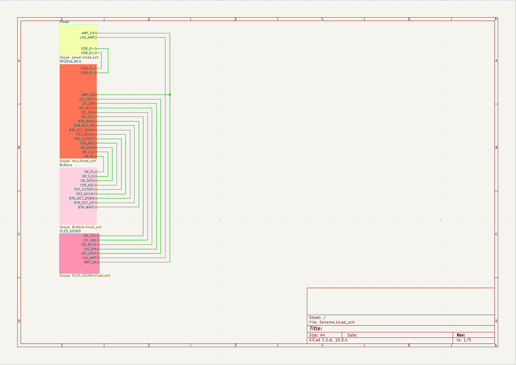
The schematic is organized in KiCad 10 across a 5-sheet hierarchical structure:
1. Root Hierarchical Overview
Provides high-level interconnection between power management, digital core, HMI inputs, and audio output stages.
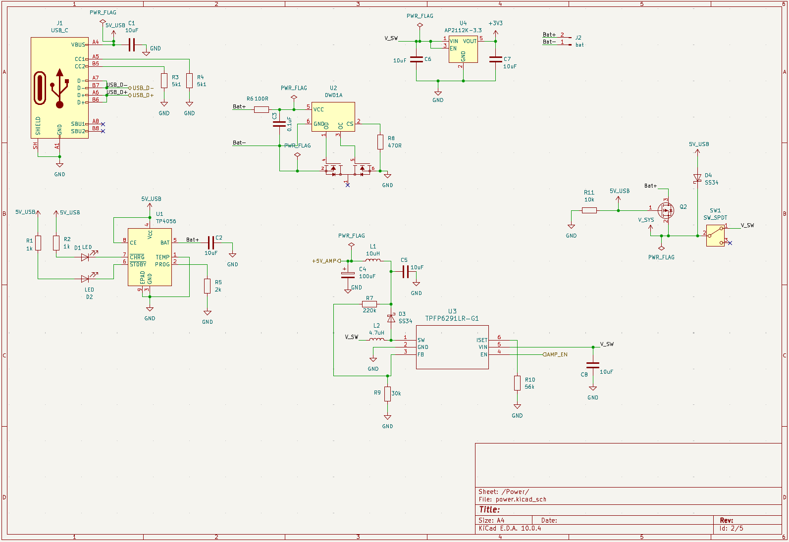
2. Power Management & Battery Subsystem
USB-C Interface (J1): Compliant CC termination resistors (R3, R4) for standard 5V/3A host detection.
TP4056 Charger (U1): Configured with $2,\text{k}\Omega$ programming resistor (R5) setting charge current to $\approx 600,\text{mA}$. Dual LED indicators for charging (D1) and standby/done (D2).
Automatic Power-Path (Q2, D4): The AO3401A P-MOSFET disconnects the Li-Po battery when USB 5V is present, powering the device directly from VBUS.
AP2112K-3.3 (U4): Ultra-low noise 600mA linear regulator feeding logic and analog reference rails.
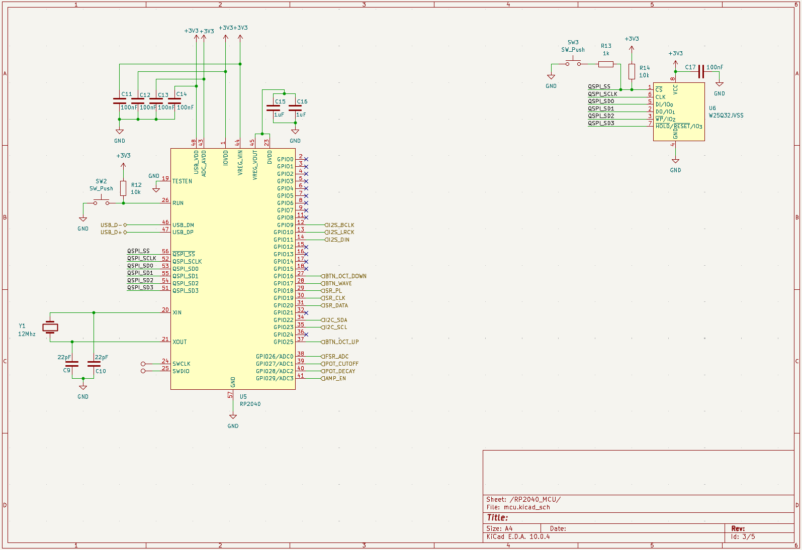
RP2040 MCU (U5): Dual ARM Cortex-M0+ silicon with individual $100,\text{nF}$ decoupling capacitors on all power pins and a $1,\mu\text{F}$ cap on internal core regulator (VREG_OUT).
Winbond W25Q32JVSS (U6): 32M-bit QSPI NOR Flash with $10,\text{k}\Omega$ pull-up (R14) and $1,\text{k}\Omega$ damping resistor (R13) on the QSPI_SS / BOOTSEL line.
Oscillator (Y1): $12.000,\text{MHz}$ crystal with dual $22,\text{pF}$ C0G/NP0 load capacitors.
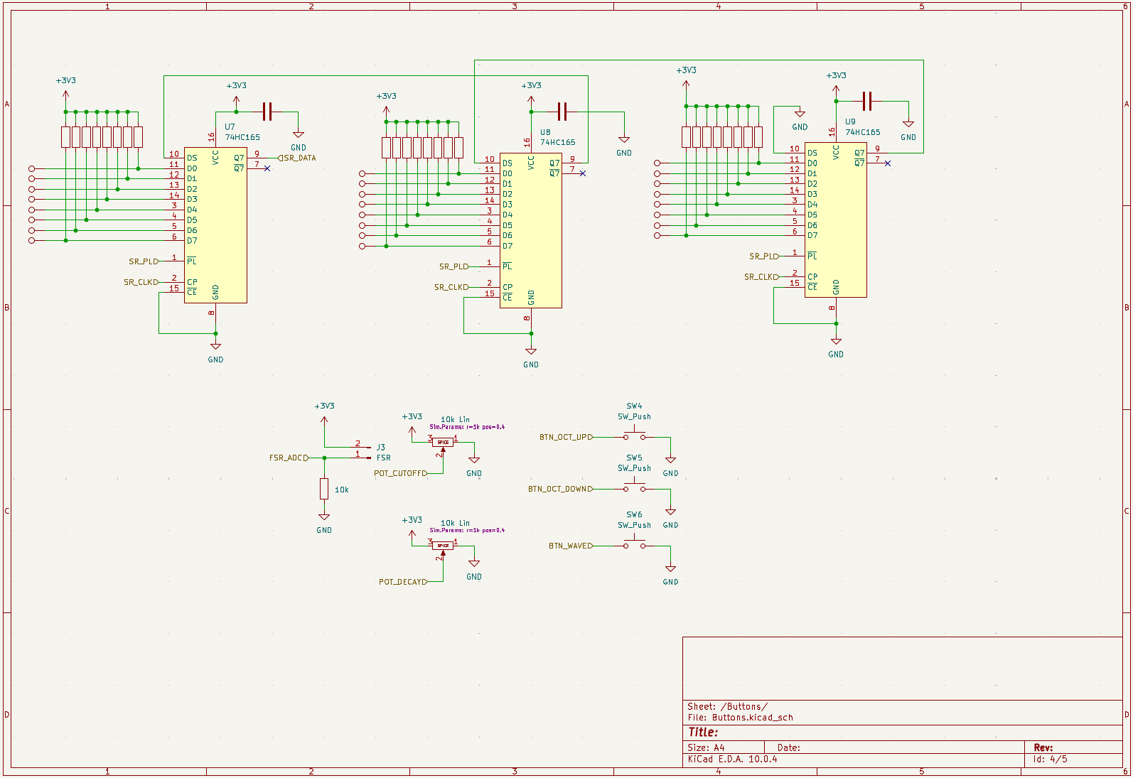
4. 24-Key Touch Matrix & HMI Controls
Shift Register Cascade: Three 74HC165 ICs (U9 $\rightarrow$ U8 $\rightarrow$ U7) multiplex 24 touch pads over a 3-wire interface (KEY_DATA, KEY_CLK, KEY_LOAD).
Pull-Up Array: Individual $10,\text{k}\Omega$ pull-ups hold all key lines at 3.3V until bridged to ground by the stylus.
Analog Controls: Potentiometers for Master Volume, Filter Cutoff (R32), and Envelope Decay (R33) connected to RP2040 12-bit ADC channels.
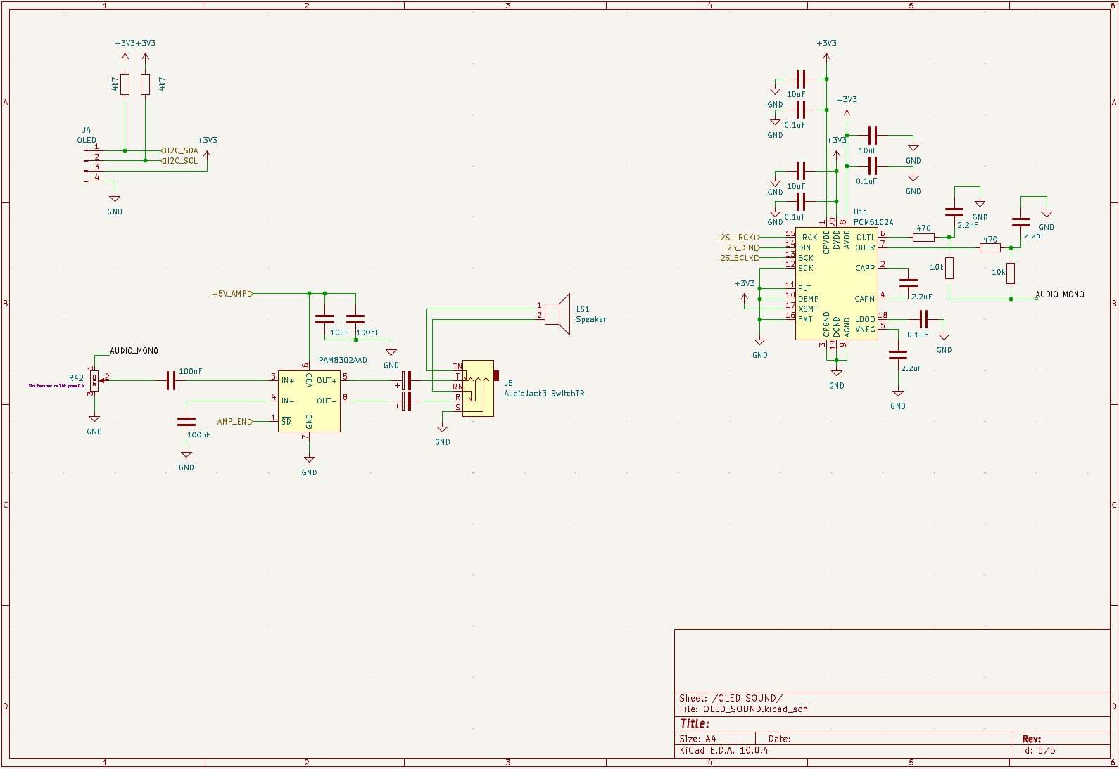
5. Audiophile DAC, Power Amp & Display
PCM5102A I2S DAC (U11): Hardware configured (SCK, DEMP, FLT, FMT to GND). Dedicated charge pump film caps produce ground-centered true bipolar output.
PAM8302A Power Stage (U10): Low-noise differential audio input with $100,\text{nF}$ AC coupling capacitors (C27, C29).
Headphone Jack (J5): CUI SJ1-3525N 3.5mm jack with switched normalling contacts.
OLED Header (J4): 4-pin I2C connector with $4.7,\text{k}\Omega$ pull-ups on SDA (GPIO0) and SCL (GPIO1).
Trace Sizing: Minimum $0.8,\text{mm} - 1.0,\text{mm}$ width for primary power trunks (+5V_AMP, V_SYS, VBAT, 5V_USB); $0.25,\text{mm}$ for high-speed digital buses.
Noise Segregation: High-frequency switching circuits (FP6291 inductor and diode) are isolated at the top edge of the board, geographically separated from the analog audio section on the left.
Firmware & Software Architecture
The OpenStylophone-RP2040 is architected to support standard RP2040 embedded toolchains:
A 3D-printable, battery-powered, USB-C rechargeable table lamp in the classic "Poldina" shape - honeycomb disc base, thin stem, down-firing cone shade with a white top - running WLED on an ESP32, with a capacitive touch…
A simple CO2 and environmental monitor based on the STM32F103C8 microcontroller. The firmware reads temperature and humidity from a DHT22 sensor, measures CO2 concentration using an MHZ19B module and displays values on…
rp2040-plus and 1.3 inch LCD screen for pi pico by waveshare
150 parts
Questions
How big is the Deneme PCB?
It measures 151 × 95 mm and has 2 copper layers, 1.6 mm thick.
What parts does the Deneme use?
143 parts, built around the RP2040, PAM8302AADCR, TPFP6291LR-G1 and W25Q32JVSSIQ. The full list of its parts is on this page, with links to each part's symbol and footprint where PCBKit's library has them.
Where can I download the Deneme KiCad files?
From the g210101021/OpenStylophone-RP2040 repository on GitHub, at the commit this page was made from: the board is hardware/Deneme.kicad_pcb and its schematic hardware/Buttons.kicad_sch. PCBKit opens the board in the browser, with nothing to install.
Can I use the Deneme design in my own project?
Its repository states no licence, so its author keeps all rights: ask g210101021 before reusing the design.


 [blocked]
 [blocked]



 Provides high-level interconnection between power management, digital core, HMI inputs, and audio output stages.