Skip to the content
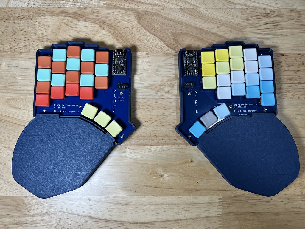
2 layers129.6 × 134.8 mmKipra kicad, the printed circuit board in 3D

A kinda pragmatic split ergonomic keyboard made with ergogen, kicad, and freecad

Size
129.6 × 134.8 mm
Copper layers
2
Thickness
1.6 mm
Parts
52
Nets
68
Pads
601
Tracks, vias
722, 1
Pours
1
Routed
Yes
KiCad
KiCad 8.0 (file 20240108)
Created
14 May 2024
Updated
1 Dec 2024

Overview

Kipra kicad is an open-source printed circuit board by focusaurus, from the focusaurus/kipra-keyboard repository on GitHub. It is a 2-layer board of 129.6 × 134.8 mm with 52 parts on 68 nets, routed with 722 tracks and 1 via.

Its parts include 22 diodes and 22 switches. It belongs with the keyboards and input boards of this library.

README

readme.md

kipra: It's kinda pragmatic.

A split ergonomic mechanical keyboard built with ergogen, kicad, and freecad.

There's a blog post with details on this build on my blog.

kipra v1

What's in this repository

  • The ergogen file at v1/kipra-v1.ergogen.yaml
  • FreeCAD files for the case, palm rest, and various jigs and smaller parts
  • The kicad PCB project files which were generated initially with ergogen then edited in kicad to route the tracks, add silkscreen, etc.
  • Some reference pinout images for the RP2040 MCU I used
  • a few screenshots from along the way
  • a zip of the gerber files I sent to PCBWay if you just want to order PCBs

Notes to self

How to make the test print

  • use ergogen via ./bin/build.sh to output v1/build/outlines/test_print.dxf
  • In freecad, start a new file and use Draft workbench
  • Import the .dxf file. It will create many shapes.
  • Select them all and hit the blue up arrow to upgrade them to wires
  • Select them all and click the squiggly icon to convert to sketch
  • Switch to Part Design Workbench
  • Make a new body
  • put the sketch in the body
  • select the sketch and pad up 6mm

MCU pinout on RP2040 (compatible)

PinUse(center)UsePin
Col ThumbP19
col innerP18
P6row 4col indexP15
P7row 3col middleP15
P8row 2col ringP16
P9row 1col pinkyP10

v1 Solder Jumpers

TL;DR this is very confusing because reversible/symmetric PCBs are confusing.

With your PCBs laid out left & right as they will be when the keyboard is built and in use - top side facing up, you solder ALL 4 COLUMNS OF JUMPERS ON THE PCB TOP SIDES. None of the jumpers on the bottom side of the PCBs get soldered.

The left and right PCBs are symmetric, but the left and right MCUs are NOT. So to account for that we have do factor that into our pinouts and jumper routing.

Info for reference:

  • In kipra v1, the footprint used was: nice_nano.js from commit 753a in github.com/ceoloide/ergogen-footprints.
  • This version did not yet support the reverse_mount parameter. If kipra v2 becomes a thing, we'll do that.
  • However, the nice_nano footprint is design with the following configuration in mind (which we do NOT want to use in the kipra):
    • you want to mount your MCUs face down (Dunno, many folks like this?)
    • you want the jumper solders on the back so they are out of sight and don't obscure the silkscreen for the MCU pinout labels
  • BUT in the case of the kipra v1, I specifically want to mount my MCUs face up because they have on-board reset buttons so flashing them is easy and I don't need a reset button on the main keyboard PCB. I added support for one just in case anyway, but hope to not have to use it. In general, I want to support the trend of the hobbyist MCUs having conveniences built-in so the barrier to build a custom keyboard is lower, and every little bit helps.

How to: model the case in FreeCad

  • start a new file
  • switch to the Draft workbench
  • import v1/build/outlines/plate-shape.dxf
  • select all the shapes in the tree view
  • click "Upgrade" blue up arrow to get a wire
  • click the wire and click the squiggly "convert birectionally from draft to sketch"
  • switch to the Part workbench
  • select the sketch and select the 2D offset (hidden behind an arrow next to 3D offset)
  • set distance to 2.6mm (2.4 for the wall and 0.2 for fit)
    • set the join type to tangent!
  • click fill offset
  • select the 2D offset in the tree view and click extrude to 10mm

How to: model the case in FreeCAD (prototype 6)

  • start a new file
  • switch to the Draft workbench
  • import v1/build/outlines/plate-shape.dxf
  • select all the shapes in the tree view
  • click "Upgrade" blue up arrow to get a wire
  • click "Upgrade" blue up arrow again to get a face
  • Use the offset 2D tool to get an offset 2.4mm from the edge of the face
    • set the join type to tangent!
  • extrude that offset up 12mm and click to make a solid
  • click the wire and click the squiggly "convert birectionally from draft to sketch"
    • this gives us the outer wall
  • extrude the face for the bottow up 2mm
  • this is all not exactly right but I was experimenting too quickly to keep track of it

Parts

52
QtyValueFootprintReferences
22ComboDiodeD1, D2, D3, D10, D11, D12, D13, D14, D15, D16, D17, D18, D19, D20, D21, D22 +6
22PG1350S1, S2, S3, S10, S11, S12, S13, S14, S15, S16, S17, S18, S19, S20, S21, S22 +6
5MountingHole_2.2mm_M2_Pad_Via_1, _2, _3, _4, _5
1E73:SW_TACT_ALPS_SKQGABE010B1
1ceoloide:nice_nanoMCU1
1TRRS-PJ-320A-dualTRRS-PJ-320A-dualTRRS1

More from focusaurus/kipra-keyboard

2
  • 2 layers159 × 120.6 mmKipra v2, the printed circuit board in 3D

    Kipra v2

    focusaurus/kipra-keyboard

    A kinda pragmatic split ergonomic keyboard made with ergogen, kicad, and freecad

    47 parts4
  • 2 layers141.7 × 117.8 mmKipra v2, the printed circuit board in 3D

    Kipra v2

    focusaurus/kipra-keyboard

    A kinda pragmatic split ergonomic keyboard made with ergogen, kicad, and freecad

    46 parts4

Similar boards

  • 2 layers41.4 × 47.5 mmU2f zero panel, the printed circuit board in 3D

    U2f zero panel

    conorpp/u2f-zero

    U2F USB token optimized for physical security, affordability, and style

    52 parts2.4k
  • 2 layers136 × 130 mmLora nodemcu, the printed circuit board in 3D

    Lora nodemcu

    sudomesh/disaster-radio

    A (paused) work-in-progress long-range, low-bandwidth wireless disaster recovery mesh network powered by the sun.

    52 parts1.1k
  • 2 layers69 × 53.8 mmTUSS4470 shield, the printed circuit board in 3D

    TUSS4470 shield

    Neumi/open_echo

    Open Source echo sounder / depth sounder / SONAR for bathymetry and research. Arduino based and compatible.

    52 parts530
  • 2 layers52.5 × 36.6 mmESP8266-WebRadio, the printed circuit board in 3D

    ESP8266-WebRadio

    karawin/Ka-Radio

    A wifi webradio with only low cost boards ESP8266 and VS1053 by Jp Cocatrix

    52 parts453
  • 2 layers105.2 × 42.4 mmRWR CONTROL PANEL, the printed circuit board in 3D

    RWR CONTROL PANEL

    jrsteensen/OpenHornet

    OpenHornet 1:1 F/A-18C Simulator Repository

    52 parts431
  • 2 layers45 × 45 mmAirCube, the printed circuit board in 3D

    AirCube

    StuckAtPrototype/AirCube

    Works standalone out of the box. Pairs with Home Assistant in minutes. Other platforms are supported through community-contributed extensions.

    52 parts379Apache-2.0
  • 2 layers160 × 99.1 mmArdumower mega shield V1.00, the printed circuit board in 3D

    Ardumower mega shield V1.00

    Ardumower/ardumower

    Develop an open source robotic lawn mower (HW+SW reference platform)

    52 parts282
  • 2 layers53 × 23 mmMaam 011109 bias, the printed circuit board in 3D

    Maam 011109 bias

    loxodes/vna

    Under development open hardware microwave vector network analyzer

    52 parts205

Questions

How big is the Kipra kicad PCB?

It measures 129.6 × 134.8 mm and has 2 copper layers, 1.6 mm thick.

What parts does the Kipra kicad use?

52 parts. The full list of its parts is on this page, with links to each part's symbol and footprint where PCBKit's library has them.

Where can I download the Kipra kicad KiCad files?

From the focusaurus/kipra-keyboard repository on GitHub, at the commit this page was made from: the board is v1/kicad/kipra-kicad.kicad_pcb and its schematic v2/kicad/kipra-v2/kipra-v2.kicad_sch. PCBKit opens the board in the browser, with nothing to install.

Can I use the Kipra kicad design in my own project?

Its repository states no licence, so its author keeps all rights: ask focusaurus before reusing the design.