
2 layers56 × 65 mm
SeaTalk1
dotnet/iot
This repo includes .NET Core implementations for various IoT boards, chips, displays and PCBs.
24 parts2.4kMIT

 finngineering/sincos_interpolator5
SinCos Interpolator to quadrature output
Sincos interpolator is an open-source printed circuit board by finngineering, from the finngineering/sincos_interpolator repository on GitHub, published under the MIT licence. It is a 2-layer board of 100 × 50 mm with 61 parts on 39 nets, routed with 393 tracks and 40 vias.
It is built around the BC557 and SF1. Its parts include 14 resistors, 10 connectors, 5 capacitors, 5 diodes and 3 ICs. It belongs with the sensors and measurement boards of this library.
The SinCos Interpolator reads the analog signals from (e.g. Heidenhain) linear scales and converts them into digital quadrature signals. The design is based on the iC-NV chip by iC-Haus. This board performs essentially the same function as Heidenhain "EXE" converters. The design was created for Heidenhain LS 403 linear scales with 11 uA peak-to-peak signals. Through different component values and solder jumper configuration, it should be usable also for other linear scales and similar transducers.
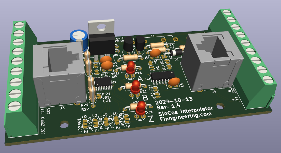
As of 2025-01-18, the latest version is 1.4 (which has RJ45 jacks rotated 180° and improved crowbar circuit, compared to version 1.3). This design has been tested to a small extent and is working. However, there appears to be reason to make some accomodations for low pass filtering of the input signals. Version 1.0 tested appeared to be otherwise working, but had power/ground swapped for the MC3487DX IC. A RJ45 jack for the encoder side has also been added since version 1.0.
By component values and solder jumper configuration, the board can be adapted to different type of transducers. For 11 uA peak-to-peak transducers, resistors R11, R12, R21 and R22 should have a 25 kOhm resistance and VREF jumpers JP11 and JP21 should be shorted by soldering. Jumper JP2/SG1 should be soldered "LO" (circuit ground) and JP1/SG0 should be left open to allow signal amplitues of up to 1 Vpp. Jumper JP5/ROT can be soldered "LO" unless some specific phase behaviour is required. Jumpers JP4/SF1 and JP3/SF0 are both left open for an interpolation factor of 5. With the 20 um periodicity of the LS 402 linear scales, this gives an output resolution of 1 um (provided the flanks of the A/B signals are "counted"). Jumper JP6/RCLK should be soldered short unless minimun transition distance needs to be adjusted. For all suggestions given in this paragraph, the iC-NV datasheet is not exceptionally clear, and you may want to do you own interpretation.
Single ended or differential outputs are selected by jumpers JP12-JP13, JP22-JP23 and JP32-JP33. In the open state, differential outputs are used, which also requires the board to be populated with the MC3487DX IC. In case single ended signals are preferred, the MC3487DX is left out and the aforementioned jumpers are soldered short. This connects the output from the iC-NV directly to the "positive" output signal terminals and the "negative" signal terminals are tied to ground.
One of the ground terminals was separated out as shield in version 1.3. This can be connected through (wihtout connecting it to ground) by soldering short JP8. Both input/output ends can also be tied to ground individually through JP7/JP9.
| Qty | Value | Footprint | References |
|---|---|---|---|
| 6 | 1k | Resistor_THT:R_Axial_DIN0207_L6.3mm_D2.5mm_P10.16mm_Horizontal | R1, R7, R8, R13, R23, R33 |
| 4 | 100n | Capacitor_THT:C_Disc_D5.0mm_W2.5mm_P2.50mm | C3, C4, C5, C6 |
| 4 | 25k | Resistor_THT:R_Axial_DIN0207_L6.3mm_D2.5mm_P2.54mm_Vertical | R11, R12, R21, R22 |
| 4 | LED | LED_THT:LED_D3.0mm | D2, D11, D21, D31 |
| 4 | MountingHole | MountingHole:MountingHole_3.2mm_M3_ISO14580 | H1, H2, H3, H4 |
| 2 | RJ45_Shielded | SinCos Interpolator Footprints:RJ45_Molex_855085001 | J3, J4 |
| 2 | SHIELD GND | Jumper:SolderJumper-2_P1.3mm_Open_RoundedPad1.0x1.5mm | JP7, JP9 |
| 1 | 100 | Resistor_THT:R_Axial_DIN0207_L6.3mm_D2.5mm_P10.16mm_Horizontal | R6 |
| 1 | 10k | Resistor_THT:R_Axial_DIN0207_L6.3mm_D2.5mm_P10.16mm_Horizontal | R5 |
| 1 | 10u | Capacitor_THT:CP_Radial_D7.5mm_P2.50mm | C1 |
| 1 | 12k | Resistor_THT:R_Axial_DIN0207_L6.3mm_D2.5mm_P10.16mm_Horizontal | R4 |
| 1 | 1N4004 | Diode_THT:D_DO-41_SOD81_P10.16mm_Horizontal | D1 |
| 1 | 500mA | Fuse:Fuseholder_Clip-5x20mm_Littelfuse_520_Inline_P20.50x5.80mm_D1.30mm_Horizontal | F1 |
| 1 | A | TerminalBlock_Phoenix:TerminalBlock_Phoenix_MKDS-1,5-2-5.08_1x02_P5.08mm_Horizontal | J12 |
| 1 | A SINGLE | Jumper:SolderJumper-2_P1.3mm_Open_RoundedPad1.0x1.5mm | JP12 |
| 1 | A- TO GND | Jumper:SolderJumper-2_P1.3mm_Open_RoundedPad1.0x1.5mm | JP13 |
| 1 | B | TerminalBlock_Phoenix:TerminalBlock_Phoenix_MKDS-1,5-2-5.08_1x02_P5.08mm_Horizontal | J22 |
| 1 | B SINGLE | Jumper:SolderJumper-2_P1.3mm_Open_RoundedPad1.0x1.5mm | JP22 |
| 1 | B- TO GND | Jumper:SolderJumper-2_P1.3mm_Open_RoundedPad1.0x1.5mm | JP23 |
| 1 | BC557 | Package_TO_SOT_THT:TO-92_Inline | Q2 |
| 1 | COS | TerminalBlock_Phoenix:TerminalBlock_Phoenix_MKDS-1,5-2-5.08_1x02_P5.08mm_Horizontal | J21 |
| 1 | COS VREF | Jumper:SolderJumper-2_P1.3mm_Open_RoundedPad1.0x1.5mm | JP21 |
| 1 | MC3487DX | Package_SO:SOIC-16_3.9x9.9mm_P1.27mm | U2 |
| 1 | POWER IN | TerminalBlock_Phoenix:TerminalBlock_Phoenix_MKDS-1,5-3-5.08_1x03_P5.08mm_Horizontal | J1 |
| 1 | POWER OUT | TerminalBlock_Phoenix:TerminalBlock_Phoenix_MKDS-1,5-3-5.08_1x03_P5.08mm_Horizontal | J2 |
| 1 | R | Resistor_THT:R_Axial_DIN0207_L6.3mm_D2.5mm_P10.16mm_Horizontal | R3 |
| 1 | RCLK | Jumper:SolderJumper-2_P1.3mm_Open_RoundedPad1.0x1.5mm | JP6 |
| 1 | ROT | Jumper:SolderJumper-3_P1.3mm_Open_RoundedPad1.0x1.5mm | JP5 |
| 1 | SF0 | Jumper:SolderJumper-3_P1.3mm_Open_RoundedPad1.0x1.5mm | JP3 |
| 1 | SF1 | Jumper:SolderJumper-3_P1.3mm_Open_RoundedPad1.0x1.5mm | JP4 |
| 1 | SG0 | Jumper:SolderJumper-3_P1.3mm_Open_RoundedPad1.0x1.5mm | JP1 |
| 1 | SG1 | Jumper:SolderJumper-3_P1.3mm_Open_RoundedPad1.0x1.5mm | JP2 |
| 1 | SHIELD CONNECT | Jumper:SolderJumper-2_P1.3mm_Open_RoundedPad1.0x1.5mm | JP8 |
| 1 | SIN | TerminalBlock_Phoenix:TerminalBlock_Phoenix_MKDS-1,5-2-5.08_1x02_P5.08mm_Horizontal | J11 |
| 1 | SIN VREF | Jumper:SolderJumper-2_P1.3mm_Open_RoundedPad1.0x1.5mm | JP11 |
| 1 | TIC116 | Package_TO_SOT_THT:TO-220-3_Vertical | Q1 |
| 1 | TL431LP | Package_TO_SOT_THT:TO-92_Inline | U3 |
| 1 | Z | TerminalBlock_Phoenix:TerminalBlock_Phoenix_MKDS-1,5-2-5.08_1x02_P5.08mm_Horizontal | J32 |
| 1 | Z SINGLE ENDED | Jumper:SolderJumper-2_P1.3mm_Open_RoundedPad1.0x1.5mm | JP32 |
| 1 | Z- TO GND | Jumper:SolderJumper-2_P1.3mm_Open_RoundedPad1.0x1.5mm | JP33 |
| 1 | ZERO | TerminalBlock_Phoenix:TerminalBlock_Phoenix_MKDS-1,5-2-5.08_1x02_P5.08mm_Horizontal | J31 |
| 1 | iC-NV | Package_SO:TSSOP-20_4.4x6.5mm_P0.65mm | U1 |
dotnet/iot
This repo includes .NET Core implementations for various IoT boards, chips, displays and PCBs.

ExploreEmbedded/8051_DevelopmentBoard
Design files and sample code for 8051 development Ultra Boards

robsonsmartins/usbflashprog
A memory device programmer (Flash/EPROM/E2PROM) board and software, connected to PC by USB port.

matthewcieplak/monotron-cv-adapter
A eurorack control voltage to Korg Monotron CV adapter board.


telec16/modular-synth
Little side project, don't expect much updates.

It measures 100 × 50 mm and has 2 copper layers, 1.6 mm thick.
61 parts, built around the BC557 and SF1. The full list of its parts is on this page, with links to each part's symbol and footprint where PCBKit's library has them.
From the finngineering/sincos_interpolator repository on GitHub, at the commit this page was made from: the board is hardware/sincos_interpolator.kicad_pcb and its schematic hardware/sincos_interpolator.kicad_sch. PCBKit opens the board in the browser, with nothing to install.
Its repository publishes it under the MIT licence: you may reuse it on that licence's terms (keep the author's notice, and for a copyleft licence share your changes alike).