2 layers44.5 × 46.9 mm
OSO SWAT B1-jig
joeycastillo/Sensor-Watch
A board replacement for the classic Casio F-91W wristwatch
31 parts2.1k
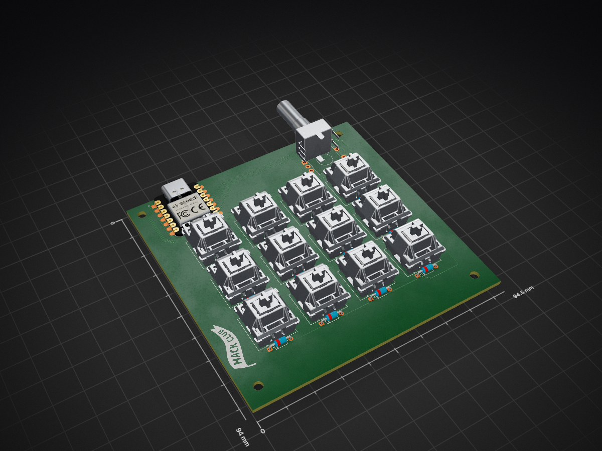
 faded-debug/Slackpad
A programmable pad that includes 12 keys used for keyboard shortcuts in apps like Slack and OBS.
Slackpad is an open-source printed circuit board by faded-debug, from the faded-debug/Slackpad repository on GitHub. It is a 2-layer board of 94.5 × 94 mm with 31 parts on 26 nets, routed with 179 tracks and 0 vias.
Its parts include 13 switches, 12 diodes and 1 IC. It belongs with the keyboards and input boards of this library.
A programmable pad that includes 12 keys used for keyboard shortcuts in apps like Slack and OBS.
| Microcontroller | Seeed XIAO RP2040 |
| Keys | 12 (4x3 switch matrix) |
| Rotary encoder | 1x EC11 with push button |
| Switches | Cherry MX compatible, 1u keycaps |
| Diodes | 12x 1N4148 (DO-35, through-hole) |
| PCB | 94.5 x 94.0 mm, 2 layers |
| Mounting | 4x M3 screws |
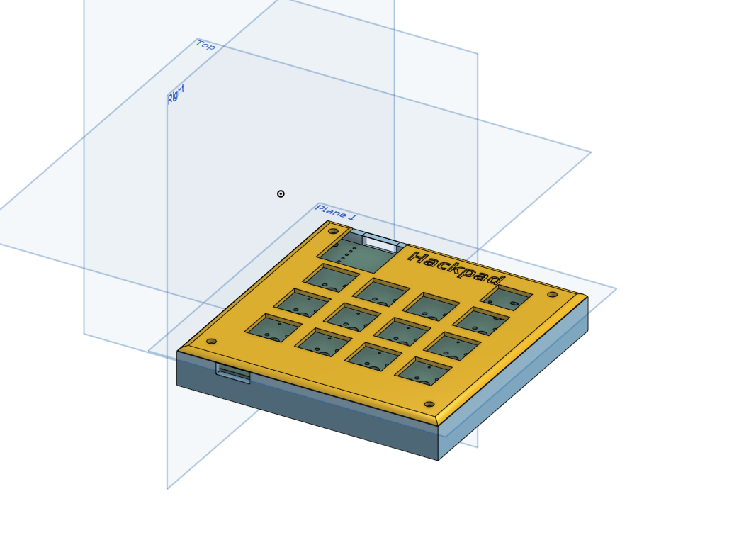
| Case | 3D printed, tray with a top plate, 99.5 x 99.0 x 14.5 mm |
| Firmware | KMK (CircuitPython) |
| Signal | XIAO pin |
|---|---|
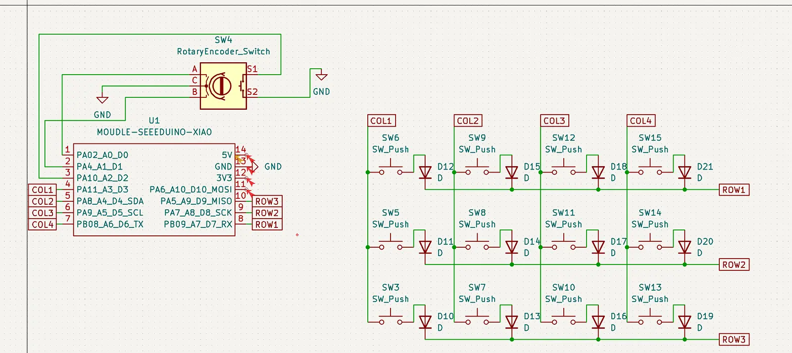
| COL1 | D3 |
| COL2 | D4 |
| COL3 | D5 |
| COL4 | D6 |
| ROW1 | D7 |
| ROW2 | D8 |
| ROW3 | D9 |
| Encoder A | D0 |
| Encoder B | D1 |
| Encoder switch | D2 |
Diode direction is COL2ROW — current flows from the column, through the
switch and its diode, into the row.
Note: on the PCB the physical columns run right to left, so COL1 is the
rightmost column.
The case is a tray with a lid. The PCB drops into the tray and is surrounded by walls on all four sides; the top plate closes it from above and carries the switches.
| Outer dimensions | 99.5 x 99.0 x 14.5 mm |
| Wall thickness | 2 mm |
| Clearance around the PCB | 0.5 mm per side |
| Space under the PCB | 3 mm, for the through-hole leads |
| Space between PCB and top plate | 3.5 mm, the Cherry MX plate mount standard |
| Top plate | 1.5 mm, 14 x 14 mm switch cutouts on a 19.05 mm grid |
The PCB rests on a 3.5 mm wide ledge that runs around the inside of the tray, and is held by 4x M3 screws that come in from underneath.
Three openings:
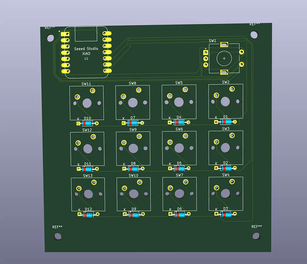
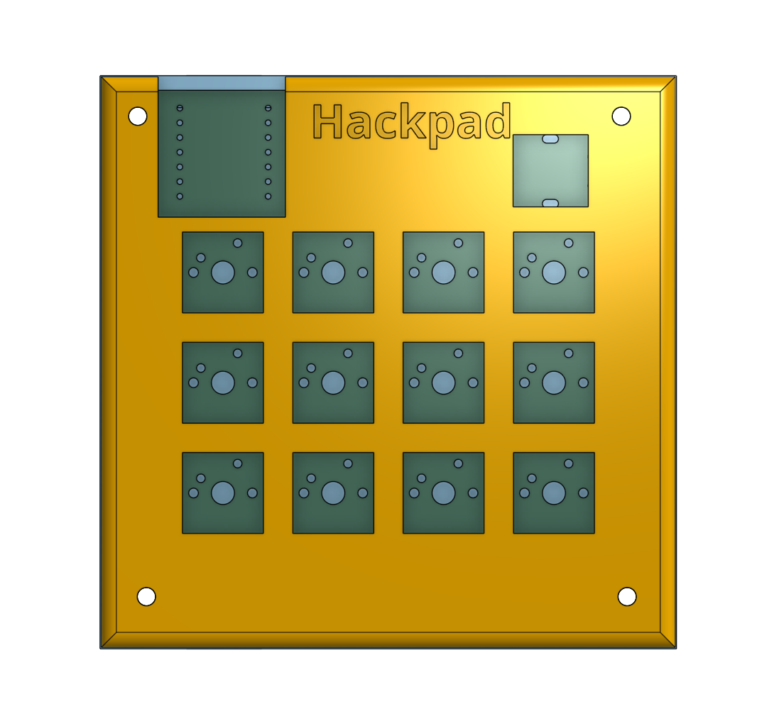
From the top, with the top plate in place. The switch cutouts, the encoder cutout and the window over the XIAO all look through onto the PCB, which sits inside the tray:
The whole thing at an angle — the tray, the wall around the PCB and the USB cutout in it:
| Part | Qty | Notes |
|---|---|---|
| Seeed XIAO RP2040 | 1 | main microcontroller |
| Cherry MX compatible switch | 12 | plate mount |
| 1u keycap | 12 | |
| 1N4148 diode | 12 | DO-35, through-hole |
| EC11 rotary encoder | 1 | with push button |
| Encoder knob | 1 | |
| M3 screw | 4 | |
| Custom PCB | 1 | 94.5 x 94.0 mm, 2 layers |
| 3D printed top plate | 1 | 1.5 mm |
| 3D printed tray | 1 | 8 mm floor with a 3 mm recess, 2 mm wall around the PCB |
The firmware is written in KMK, which runs on CircuitPython.
To flash it:
.uf2 onto the RPI-RP2 drive that appears.kmk folder from the KMK repository onto the CIRCUITPY drive.Firmware/main.py onto the CIRCUITPY drive.Editing the keymap only means editing main.py and saving it — no compiling.
| Folder | Contents |
|---|---|
CAD/ | complete case model in STEP format, including the PCB |
PCB/ | KiCad project: schematic, board and footprint library |
Firmware/ | KMK firmware source |
Production/ | everything needed to actually make one: STLs, firmware, gerbers |
images/ | screenshots used in this README |
Production/ holds the files you send to a fab house or a printer:
| File | What it is |
|---|---|
gerbers.zip | 2 copper layers, both silkscreens, both solder masks, edge cuts, and separate PTH/NPTH Excellon drill files |
Bottom plate.stl | the tray, 99.5 x 99.0 x 13 mm |
Top plate.stl | the top plate |
firmware/ | CircuitPython .uf2 for the XIAO RP2040, plus the kmk library and main.py that go onto the CIRCUITPY drive |
KMK runs on CircuitPython, so there is no binary to compile — the .uf2 is the
runtime and the two Python files are the keyboard. Together they are the
flashable firmware.
| Qty | Value | Footprint | References |
|---|---|---|---|
| 12 | D | Diode_THT:D_DO-35_SOD27_P7.62mm_Horizontal | D1, D2, D3, D4, D5, D6, D7, D8, D9, D10, D11, D12 |
| 12 | SW_Push | Button_Switch_Keyboard:SW_Cherry_MX_1.00u_PCB | SW2, SW3, SW4, SW5, SW6, SW7, SW8, SW9, SW10, SW11, SW12, SW13 |
| 1 | LOGO | footprints:flaga3 | G*** |
| 1 | MOUDLE-SEEEDUINO-XIAO | footprints:XIAO-Generic-Hybrid-14P-2.54-21X17.8MM | U1 |
| 1 | RotaryEncoder_Switch | Rotary_Encoder:RotaryEncoder_Alps_EC11E-Switch_Vertical_H20mm | SW1 |
The 27 most common of 31 parts.
It measures 94.5 × 94 mm and has 2 copper layers, 1.6 mm thick.
31 parts. The full list of its parts is on this page, with links to each part's symbol and footprint where PCBKit's library has them.
From the faded-debug/Slackpad repository on GitHub, at the commit this page was made from: the board is PCB/Slackpad.kicad_pcb and its schematic PCB/Slackpad.kicad_sch. PCBKit opens the board in the browser, with nothing to install.
Its repository states no licence, so its author keeps all rights: ask faded-debug before reusing the design.
joeycastillo/Sensor-Watch
A board replacement for the classic Casio F-91W wristwatch

hoglet67/RGBtoHDMI
Bare-metal Raspberry Pi project that provides pixel-perfect sampling of Retro Computer RGB/YUV video and conversion to HDMI

hackclub/OnBoard
💡 Join 1,000 teenagers and make your first PCB with a $100 grant!

openwch/ch32v003
CH32V003 is an ultra-cheap RISC-V MCU with 2KB SRAM, 16KB flash, and up to 18 GPIOs that sells for under $0.10

Luos-io/luos_engine
Open-source and real-time orchestrator for cyber-physical-systems, to easily design, test and deploy embedded applications and digital twins.

BlueAndi/Pixelix
Full RGB LED matrix, based on an ESP32 and WS2812B LEDs or emulated LEDs on TFT.

