2 layers50.8 × 107.9 mm
 F9Motion/keeb
Custom mechanical keyboard project for Hack Club Keeb
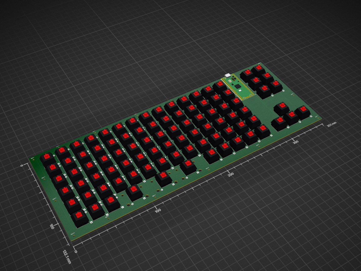
Keeb is an open-source printed circuit board by F9Motion, from the F9Motion/keeb repository on GitHub. It is a 2-layer board of 351 × 132.1 mm with 202 parts on 149 nets, routed with 608 tracks and 31 vias.
Its parts include 91 diodes and 91 switches. It belongs with the keyboards and input boards and the RP2040 boards of this library.
Custom mechanical keyboard project for Hack Club Keeb
I got interested in building this custom keyboard because I'm passionate about workplace setups and desk aesthetics. By trade, I'm a Motion Designer (I mainly work in Adobe After Effects), but the process of creating a custom keyboard completely sucked me in. Now, I definitely want to keep building custom hardware in the future!
When I first found out about the Hack Club grant, I wanted to put everything into this board — OLED screens, a volume knob, and RGB LEDs. However, once I started routing the traces on the PCB, things got messy very fast. I simply ran out of space.
To overcome these issues and avoid the hassle of sourcing and tuning stabilizers, I redesigned the layout to use three short spacebars instead of a standard long one.
While working on the PCB, I placed the screw mounts and initially didn't notice that the Pico's USB-C connector ended up stuck right in the middle of the board! I had to go back to KiCad and re-route the traces to fix the connector placement.
At first, I tried to design the case using Onshape, but I found its workflow very uncomfortable for my style — to the point where I almost gave up and deleted the progress. But then I realized I could use Blender, a program I already knew well from rendering my first 3D short film. Switching to Blender allowed me to finish the case design smoothly and separate the top plate for a clean print.
All PCB routing, case files, and firmware are finalized. I can't wait to get the parts printed and manufactured so I can assemble this keyboard and use it in my daily setup!
| Qty | Value | Footprint | References |
|---|---|---|---|
| 91 | 1.5KExxA | Diode_THT:D_DO-201AE_P15.24mm_Horizontal | D1, D2, D10, D11, D12, D13, D14, D15, D16, D17, D18, D19, D20, D21, D22, D23 +75 |
| 91 | SW_Push | Button_Switch_Keyboard:SW_Cherry_MX_1.00u_PCB | SW1, SW2, SW10, SW11, SW12, SW13, SW14, SW15, SW16, SW17, SW18, SW19, SW20, SW21, SW22, SW23 +75 |
| 1 | RaspberryPi_Pico | Module:RaspberryPi_Pico_Common_Unspecified | A1 |
The 183 most common of 202 parts.
It measures 351 × 132.1 mm and has 2 copper layers, 1.6 mm thick.
202 parts. The full list of its parts is on this page, with links to each part's symbol and footprint where PCBKit's library has them.
From the F9Motion/keeb repository on GitHub, at the commit this page was made from: the board is keeb.kicad_pcb and its schematic keeb.kicad_sch. PCBKit opens the board in the browser, with nothing to install.
Its repository states no licence, so its author keeps all rights: ask F9Motion before reusing the design.

drpykachu/Sonar-Watch
A self-designed, home-made watch intended to tell time in a funky and unique way!


Thinkpad4by3/chibitron
Electrostatic CRT driver designed from the ground up for performance, versatility and ease-of-manufacturability


lens42/D-Lev-All-in-One-PCB
This integrates the excellent D-Lev digital theremin design at D-Lev.com into a single surface mount PCB

GadgetReboot/Low_Side_Switch
16 channel low-side switch for driving resistive/inductive loads