Skip to the content
PCBKitNew board
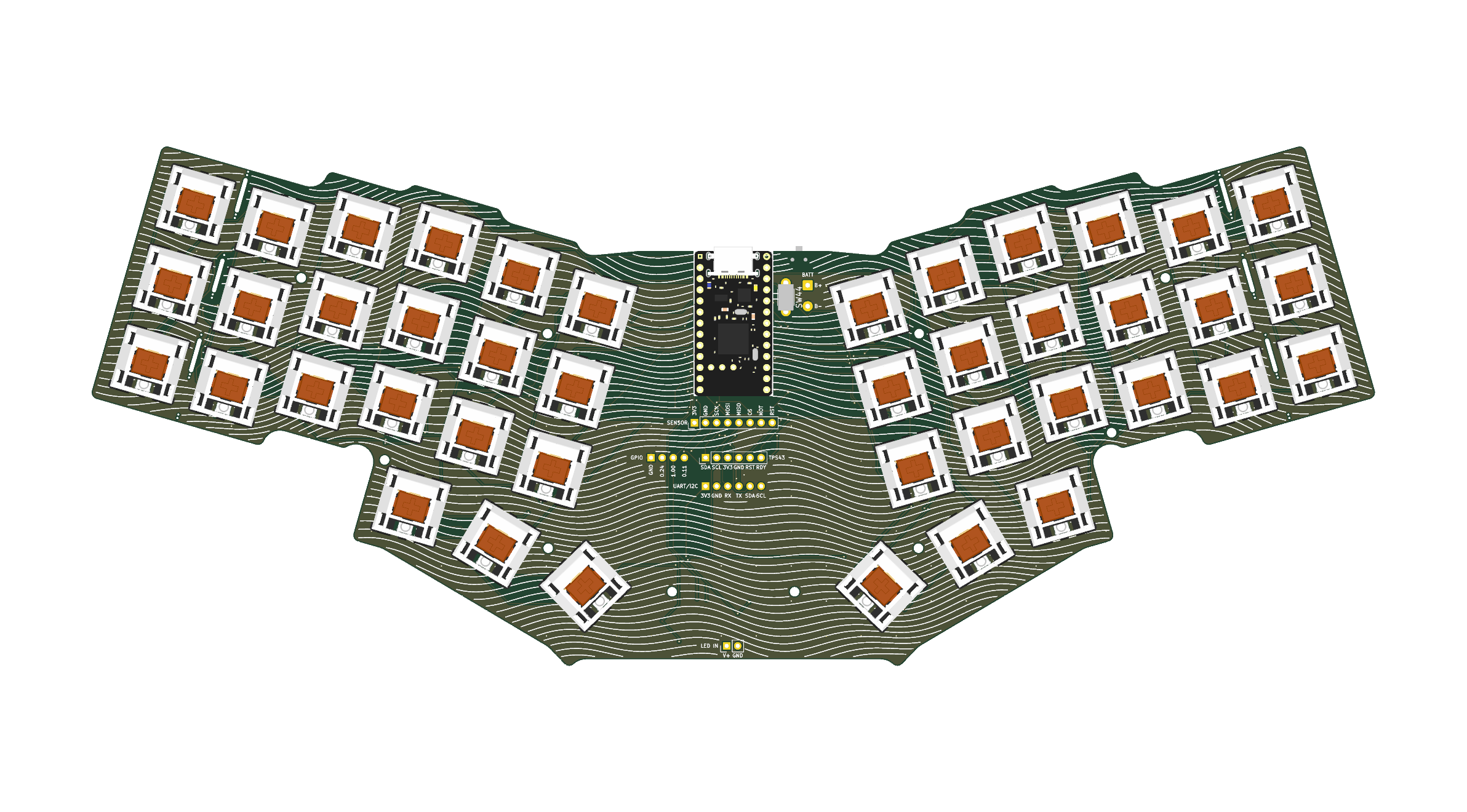
2 layers293.4 × 118.8 mmUnicorne, the printed circuit board in 3D

A unibody Corne: both halves of the Corne v3 key layout on one PCB, each half rotated 16°, with an Azoteq TPS43 trackpad in the middle (it sits on the case, over the nice!nano) and a nice!nano v2 at the top.

Size
293.4 × 118.8 mm
Copper layers
2
Thickness
1.6 mm
Parts
175
Nets
130
Pads
732
Tracks, vias
2,736, 451
Pours
2
Routed
Yes
KiCad
KiCad 10.0 (file 20260206)
Created
24 Oct 2026
Updated
27 Oct 2026

Overview

Unicorne is an open-source printed circuit board by EyalYe, from the EyalYe/unicorne repository on GitHub. It is a 2-layer board of 293.4 × 118.8 mm with 175 parts on 130 nets, routed with 2,736 tracks and 451 vias.

It is built around the SN74LV1T125DBV, 1N4148W and SK6812MINI-E, with the AO3401A among its other parts. Its parts include 96 diodes, 44 switches, 6 connectors, 5 resistors and 2 capacitors. It belongs with the nRF52 and nRF5x boards of this library.

Main components

4

README

README.md

unicorne

A unibody Corne: both halves of the Corne v3 key layout on one PCB, each half rotated 16°, with an Azoteq TPS43 trackpad in the middle (it sits on the case, over the nice!nano) and a nice!nano v2 at the top.

Status: layout fixed, schematic done, MX and Choc boards fully routed (DRC: 0 unconnected, 0 copper violations).

Design

  • 42 keys (3×6 + 3 thumbs per half), outer pinky columns break off for a 36-key board

  • Key spacing, stagger, thumb cluster and LED positions copied from crkbd v3-final (19.0 mm pitch)

  • Two board versions with the same placement: Kailh MX hotswap, and Kailh Choc hotswap (fits Choc V1 and V2)

  • nice!nano v2 on the top side, components up, USB on the top edge; the edge is notched for the mid-mount USB-C, whose shell drops below the nano's underside

  • TPS43 trackpad wired to six bare pads (no FPC, to keep it thin). It sits on the case above the board, so it may cover the nice!nano; its position is the one that brings the halves closest together (higher and it meets the inner columns' top keycaps, lower and the thumb keycaps). It is drawn on F.Fab and User.Drawings only, with no 3D model on the board

  • Optional LEDs: 12 SK6812MINI underglow + 42 SK6812MINI-E per key, on their own MOSFET-switched supply. A solder jumper picks the source: the nice!nano's 3.3 V VCC (up to its 1 A regulator), or an external supply up to 5 V on the LED IN pads for full brightness. Never the battery.

  • MSK-12C02 battery cut-off switch, through-hole battery pads

  • Exposed pads: expansion header (3V3, GND, UART, I2C) and GPIO header (P0.24, P1.00, P0.11)

  • Pro Micro mode: a Pro Micro-footprint controller without the nice!nano's three inner pins (P1.01, P1.02, P1.07) works with three solder jumpers bridged, which move those nets to outer pins that aren't the Pro Micro I2C pair:

    JumperNet (nice!nano pin)Bridged toThat pin's other use, lost in this mode
    JP4COL5 (P1.01)P0.24free GPIO / sensor MISO
    JP5COL6 (P1.02)P0.11free GPIO / sensor CS
    JP6ROW5 (P1.07)P0.08UART RX

    I2C (SDA/SCL), the trackpad's RDY, LED data (P0.06) and LED power (P1.00) keep working. Leave all three open with a nice!nano, or two controller pins drive one net. In firmware, point COL5, COL6 and ROW5 at the bridged pins.

The full pin plan and parts list are in mock/index.html (open it in a browser).

Parts list

Everything is hand-soldered. Quantities are for one board; the 36-key build needs 36 of each per-key part.

On the PCB

RefQtyPartFootprintNotes
U11nice!nano v2through-hole, top sideNeeds the 3 inner pads (P1.01, P1.02, P1.07) too; use low-profile sockets or solder directly
SW1–4242Key switches: MX, or Choc V1/V2hotswapMX on unicorne.kicad_pcb, Choc on unicorne-choc.kicad_pcb
—42Hotswap sockets: Kailh MX, or Kailh ChocSMD, bottomThe Choc socket fits both V1 and V2 switches
D1–42421N4148W diodeSOD-123, bottom
SW431MSK-12C02 slide switchSMD, bottom, top edgeBattery cut-off
SW441TS-1136 H4.3 tactile switch (6.0×3.5 mm, 4.3 mm tall, 2 pins)through-hole, top, beside the nanoReset
J1—Battery B+ / B− padsthrough-hole, 4.8 mmSolder the battery leads here
J2—TPS43 padsthrough-hole, 2.54 mmWires to the trackpad (trackpad build)
J5—Sensor padsthrough-hole, 2.54 mmWires to a PAW3395 / PMW3360 board (sensor build)
J311×6 pin header, 2.54 mmthrough-holeOptional: expansion (3V3, GND, UART, I2C)
J411×4 pin header, 2.54 mmthrough-holeOptional: GPIO (P0.24, P1.00, P0.11)
R3, R424.7 kΩ resistor0603 hand-solderTrackpad build only (I2C pull-ups); leave off with a sensor
R5110 kΩ resistor0603 hand-solderTrackpad / sensor reset pull-up

Optional LEDs

Leave all of these off for a board without lighting.

RefQtyPartFootprintNotes
LED1–1212SK6812MINI3.5 mm PLCC4, bottomUnderglow
LED13–5442SK6812MINI-Ereverse mount, bottomPer-key; shines up through a cutout
JP2—3-pad solder jumper—LED source: bridge VCC–centre, or EXT–centre for J6
J6—LED IN pads (V+, GND)through-hole, 2.54 mmExternal LED supply up to 5 V, e.g. a USB-C breakout; only with JP2 on EXT
Q11AO3401A P-MOSFETSOT-23Switches the LED supply
Q212N7002 N-MOSFETSOT-23Driven by P1.00
R1, R22100 kΩ resistor0603 hand-solderKeep the LEDs off during boot
C1110 µF capacitor0603 hand-solderLED supply
U21SN74LV1T125 bufferSOT-23-5 hand-solderLED data level shifter, needed only with JP2 on EXT; must be the LV1T (not 74LVC1G125) so 3.3 V data works at 5 V
C21100 nF capacitor0603 hand-solderU2 decoupling; leave off with U2
JP3—Solder jumper—U2 bypass: bridge it with JP2 on VCC and U2 left off
JP1—Solder jumper—Bridge it to send LED data from P0.06 (through U2)
JP4–JP6—Solder jumpers—Pro Micro mode only: bridge all three without a nice!nano; open with one

Off the PCB

QtyPartNotes
1Azoteq TPS43 trackpad (43.3 × 40.3 mm)Trackpad build; or a PAW3395 / PMW3360 sensor board for a trackball (3.3 V supply)
13.7 V LiPo batterySits under the trackpad on the bottom; size it to your case
42Keycaps, MX or Choc40 × 1u and 2 × 1.5u (the big thumb key on each half)
10M2 button-head screws (ISO 7380) + standoffsMounting holes H1–H10; standoff height depends on the case

Ordering (JLCPCB)

Upload export/jlcpcb/unicorne-mx-jlcpcb.zip or unicorne-choc-jlcpcb.zip (gerbers plus Excellon drills, plated and non-plated separate). Settings:

OptionValue
Layers2
Thickness1.6 mm
Sizeabout 293 × 119 mm (read from the outline)
Min. via / hole0.3 mm via drill, 0.5 mm mouse-bite holes
Min. track / spacing0.2 mm / 0.2 mm (0.15 mm rule minimum)
Surface finishHASL (lead-free if you prefer)
Everything elsedefaults

No assembly: every part is hand-soldered (see the parts list). Regenerate the zips with python3 tools/export_gerbers.py after any board change; it refuses to export a board that fails DRC.

3D

export/unicorne-mx.step and export/unicorne-choc.step are the full boards with parts, for designing a case (rendered previews next to them). Sockets and the Cherry MX and Choc V1 switches are real models; the nice!nano, TPS43, SK6812MINI and MSK-12C02 are size-accurate placeholder boxes from tools/step_box.py. Regenerate with python3 tools/export_3d.py after any board change.

MX board

Switch plates

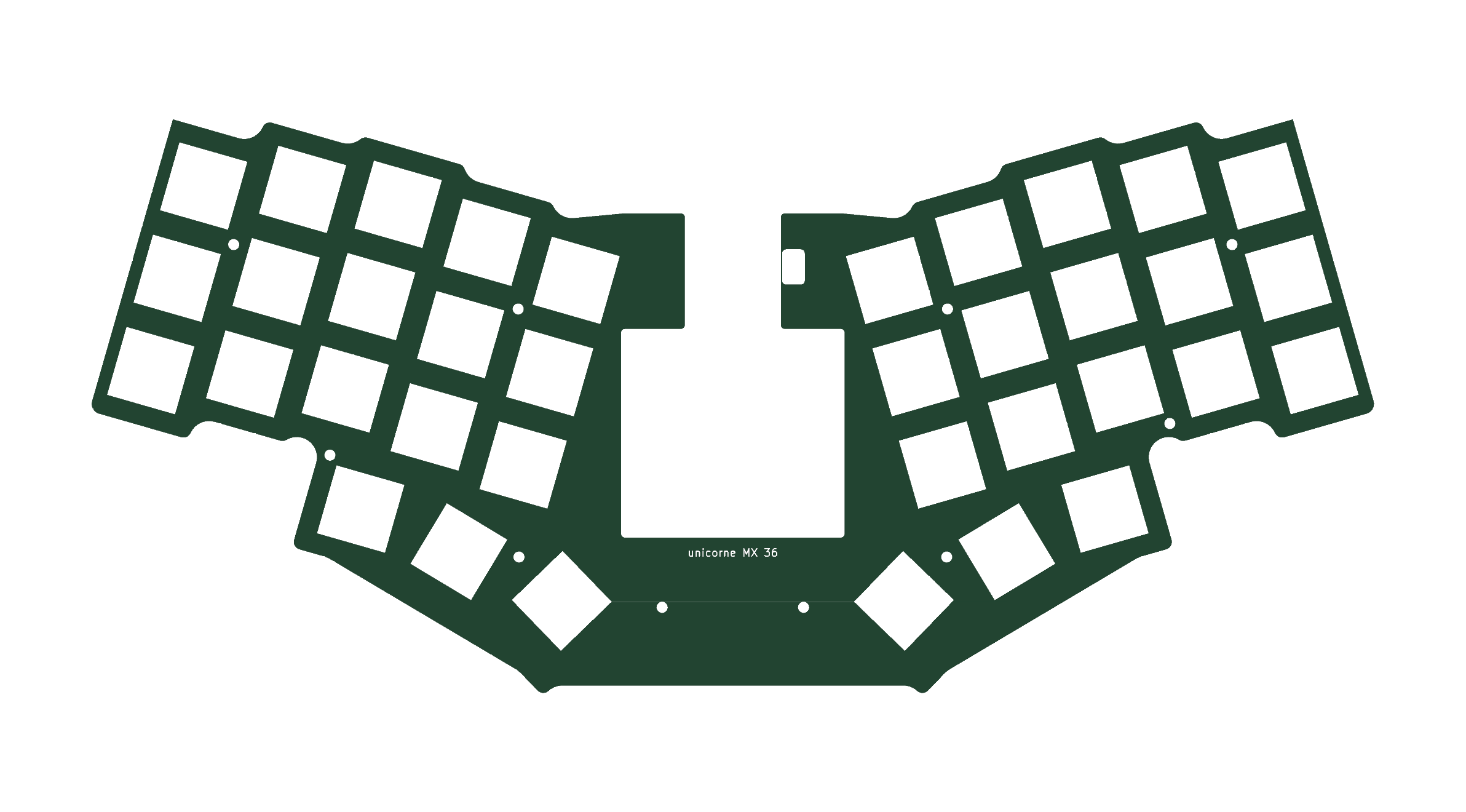
The top plate, as a starting point for a case. Plates are solid (no break lines), so there is one per switch type and size:

PlateCutoutsThickness
plate/unicorne-mx-42-plate.kicad_pcb, plate/unicorne-mx-36-plate.kicad_pcb14.0 mm1.5 mm
plate/unicorne-choc-42-plate.kicad_pcb, plate/unicorne-choc-36-plate.kicad_pcb13.8 mm1.2 mm

Each has the same outline, coordinates and M2 holes as its PCB, a 44.3 x 41.3 mm opening for the TPS43, an opening over the nice!nano that runs out through the top edge (so the USB stays reachable) and a window over the reset switch, both with 0.5 mm clearance. The 36-key plates are cut evenly on both sides where the PCB snaps off its outer columns (on Choc, whose break lines differ by side, at their average), with rounded corners. export/plate/ holds, per plate:

  • *-jlcpcb.zip: order as an FR4 board, no copper (the copper layers are included empty so JLCPCB's viewer reads the stack); set the thickness above.
  • *.dxf: Edge.Cuts outline in mm, for laser-cut aluminium, steel or acrylic.
  • *.step: the plate solid, in the same coordinates as the board STEP files.
  • *.png: a render.

MX 36-key plate

Files

PathContents
unicorne.kicad_proKiCad 10 project
unicorne.kicad_sch, matrix.kicad_sch, leds.kicad_schSchematic (generated, see below)
unicorne.kicad_pcbMX hotswap PCB (generated, see below)
unicorne-choc.kicad_pcb, unicorne-choc.kicad_proChoc V1/V2 hotswap PCB, same placement
unicorne.kicad_druExtra DRC rules (LED cutout edge clearance)
lib/Project symbols and footprints; third-party credits in lib/ATTRIBUTION.md
tools/fp_tactile.pyGenerates the reset switch footprint
tools/layout.pyKey, trackpad and outline geometry → mock/layout.json, mock/unicorne.svg
tools/gen_schematic.pyGenerates the schematic sheets from mock/layout.json
tools/gen_pcb.pyBuilds both PCBs from the schematic netlist and mock/layout.json
tools/krt_route.pyRoutes a freshly generated board (used for both boards): fixed lanes, then KiCadRoutingTools 0.23.7 for every other signal at standard JLCPCB sizes with no via in or next to a pad, the maze router for anything left, GND pours and stitching, then its plane repair. Expects KiCadRoutingTools in ~/Development/tools/KiCadRoutingTools with its own venv
tools/finish_route.pyThe older all-in-house router: fixed lanes, then KiCad's ratsnest with the maze router, GND pours and stitching; up to 10 attempts, then GND repair and stub cleanup. Also keeps new vias out of pads
tools/gnd_repair.pyFinds GND copper the pours left cut off and joins it (a via, or rip-up and reroute of whatever boxes it in)
tools/lanes.py, tools/maze_route.pyFixed routing lanes for the key grid; the grid A* router
tools/route.pyFreerouting driver (not used for the final boards)
tools/step_box.py, lib/3d/Placeholder STEP models and the socket / Choc switch models
tools/export_3d.py, export/STEP export of both boards, and 3D renders
tools/export_gerbers.py, export/jlcpcb/JLCPCB gerber + drill zips
docs/led-map.md, docs/led-map.csvEvery LED's index in the data chain (0-based, for firmware), its reference, spot and the key's matrix row and column
tools/led_map.pyGenerates the LED map from the board
tools/led_order.jsonThe LED chain order, picked in the LED Chain Order page; gen_schematic.py uses it when present
tools/waves.pyWavy silkscreen pattern on both sides of the routed PCBs
tools/gen_plate.py, plate/, export/plate/42- and 36-key switch plates and their exports
mock/Layout data, a 1:1 printable SVG and the design overview page

Regenerating

sh
# Geometry (needs KiCad's bundled Python for the outline)
/Applications/KiCad/KiCad.app/Contents/Frameworks/Python.framework/Versions/Current/bin/python3 tools/layout.py

# Schematic (overwrites the three .kicad_sch files)
python3 tools/gen_schematic.py

# PCBs (overwrite the board files; placement, outline, holes, silkscreen, no tracks)
# then route them; both steps throw away any hand routing
/Applications/KiCad/KiCad.app/Contents/Frameworks/Python.framework/Versions/Current/bin/python3 tools/gen_pcb.py mx
/Applications/KiCad/KiCad.app/Contents/Frameworks/Python.framework/Versions/Current/bin/python3 tools/gen_pcb.py choc
/Applications/KiCad/KiCad.app/Contents/Frameworks/Python.framework/Versions/Current/bin/python3 tools/krt_route.py mx
/Applications/KiCad/KiCad.app/Contents/Frameworks/Python.framework/Versions/Current/bin/python3 tools/krt_route.py choc
# On MX the plane repair reaches U2 pad 3 (GND, boxed in by LED_DIN) only through a via in the
# pad, which krt_route.py removes, leaving that pad unconnected. The committed board joins it by
# hand: a via at (160.65, 137.45) between pads 3 and 4, a back-layer track to pad 3 and a
# front-layer track to the GND copper.

# LED map for firmware (chain index -> LED, switch, matrix position)
/Applications/KiCad/KiCad.app/Contents/Frameworks/Python.framework/Versions/Current/bin/python3 tools/led_map.py

# Wavy silkscreen on both PCBs (redraws only the waves, leaves the routing alone)
/Applications/KiCad/KiCad.app/Contents/Frameworks/Python.framework/Versions/Current/bin/python3 tools/waves.py

# Switch plates and their exports (reads hole positions from the routed boards)
/Applications/KiCad/KiCad.app/Contents/Frameworks/Python.framework/Versions/Current/bin/python3 tools/gen_plate.py

Licenses

The nice!nano footprint comes from bstiq/nice-nano-kicad under GPLv3; the hotswap footprints from keyswitch-kicad-library under MIT.

Parts

175
QtyValueFootprintReferences
421N4148WDiode_SMD:D_SOD-123D1, D2, D10, D11, D12, D13, D14, D15, D16, D17, D18, D19, D20, D21, D22, D23 +26
42SK6812MINI-ELED_SMD:LED_SK6812MINI-E_3.2x2.8mm_P1.5mm_ReverseMountLED1, LED2, LED10, LED12, LED14, LED15, LED16, LED17, LED19, LED20, LED21, LED22, LED24, LED25, LED27, LED28 +26
12SK6812MINIunicorne:LED_SK6812MINI_PLCC4_3.5x3.5mm_P1.75mmLED4, LED8, LED11, LED13, LED18, LED23, LED26, LED29, LED37, LED40, LED45, LED47
10M2MountingHole:MountingHole_2.2mm_M2_ISO7380H1, H2, H3, H4, H5, H6, H7, H8, H9, H10
2100kResistor_SMD:R_0603_1608Metric_Pad0.98x0.95mm_HandSolderR1, R2
24.7kResistor_SMD:R_0603_1608Metric_Pad0.98x0.95mm_HandSolderR3, R4
2mouse bitesMB1, MB2
1100nFCapacitor_SMD:C_0603_1608Metric_Pad1.08x0.95mm_HandSolderC2
110kResistor_SMD:R_0603_1608Metric_Pad0.98x0.95mm_HandSolderR5
110uFCapacitor_SMD:C_0603_1608Metric_Pad1.08x0.95mm_HandSolderC1
12N7002Package_TO_SOT_SMD:SOT-23Q2
1AO3401APackage_TO_SOT_SMD:SOT-23Q1
1BatteryConnector_Wire:SolderWire-0.5sqmm_1x02_P4.8mm_D0.9mm_OD2.3mmJ1
1COL5 to P0.24Jumper:SolderJumper-2_P1.3mm_Open_RoundedPad1.0x1.5mmJP4
1COL6 to P0.11Jumper:SolderJumper-2_P1.3mm_Open_RoundedPad1.0x1.5mmJP5
1ExpansionConnector_PinHeader_2.54mm:PinHeader_1x06_P2.54mm_VerticalJ3
1GPIOConnector_PinHeader_2.54mm:PinHeader_1x04_P2.54mm_VerticalJ4
1LED dataJumper:SolderJumper-2_P1.3mm_Open_RoundedPad1.0x1.5mmJP1
1LED power inConnector_PinHeader_2.54mm:PinHeader_1x02_P2.54mm_VerticalJ6
1LED sourceJumper:SolderJumper-3_P1.3mm_Open_RoundedPad1.0x1.5mmJP2
1PAW3395 / PMW3360Connector_PinHeader_2.54mm:PinHeader_1x08_P2.54mm_VerticalJ5
1Powerunicorne:SW_SPDT_Shouhan_MSK12C02SW43
1R0C0unicorne:SW_Hotswap_Kailh_MX_1.00uSW1
1R0C1unicorne:SW_Hotswap_Kailh_MX_1.00uSW2
1R0C2unicorne:SW_Hotswap_Kailh_MX_1.00uSW3
1R0C3unicorne:SW_Hotswap_Kailh_MX_1.00uSW4
1R0C4unicorne:SW_Hotswap_Kailh_MX_1.00uSW5
1R0C5unicorne:SW_Hotswap_Kailh_MX_1.00uSW6
1R0C6unicorne:SW_Hotswap_Kailh_MX_1.00uSW19
1R1C0unicorne:SW_Hotswap_Kailh_MX_1.00uSW7
1R1C1unicorne:SW_Hotswap_Kailh_MX_1.00uSW8
1R1C2unicorne:SW_Hotswap_Kailh_MX_1.00uSW9
1R1C3unicorne:SW_Hotswap_Kailh_MX_1.00uSW10
1R1C4unicorne:SW_Hotswap_Kailh_MX_1.00uSW11
1R1C5unicorne:SW_Hotswap_Kailh_MX_1.00uSW12
1R1C6unicorne:SW_Hotswap_Kailh_MX_1.00uSW20
1R2C0unicorne:SW_Hotswap_Kailh_MX_1.00uSW13
1R2C1unicorne:SW_Hotswap_Kailh_MX_1.00uSW14
1R2C2unicorne:SW_Hotswap_Kailh_MX_1.00uSW15
1R2C3unicorne:SW_Hotswap_Kailh_MX_1.00uSW16
1R2C4unicorne:SW_Hotswap_Kailh_MX_1.00uSW17
1R2C5unicorne:SW_Hotswap_Kailh_MX_1.00uSW18
1R2C6unicorne:SW_Hotswap_Kailh_MX_1.50uSW21
1R3C0unicorne:SW_Hotswap_Kailh_MX_1.00uSW22
1R3C1unicorne:SW_Hotswap_Kailh_MX_1.00uSW23
1R3C2unicorne:SW_Hotswap_Kailh_MX_1.00uSW24
1R3C3unicorne:SW_Hotswap_Kailh_MX_1.00uSW25
1R3C4unicorne:SW_Hotswap_Kailh_MX_1.00uSW26
1R3C5unicorne:SW_Hotswap_Kailh_MX_1.00uSW27
1R3C6unicorne:SW_Hotswap_Kailh_MX_1.00uSW40
1R4C0unicorne:SW_Hotswap_Kailh_MX_1.00uSW28
1R4C1unicorne:SW_Hotswap_Kailh_MX_1.00uSW29
1R4C2unicorne:SW_Hotswap_Kailh_MX_1.00uSW30
1R4C3unicorne:SW_Hotswap_Kailh_MX_1.00uSW31
1R4C4unicorne:SW_Hotswap_Kailh_MX_1.00uSW32
1R4C5unicorne:SW_Hotswap_Kailh_MX_1.00uSW33
1R4C6unicorne:SW_Hotswap_Kailh_MX_1.00uSW41
1R5C0unicorne:SW_Hotswap_Kailh_MX_1.00uSW34
1R5C1unicorne:SW_Hotswap_Kailh_MX_1.00uSW35
1R5C2unicorne:SW_Hotswap_Kailh_MX_1.00uSW36
1R5C3unicorne:SW_Hotswap_Kailh_MX_1.00uSW37
1R5C4unicorne:SW_Hotswap_Kailh_MX_1.00uSW38
1R5C5unicorne:SW_Hotswap_Kailh_MX_1.00uSW39
1R5C6unicorne:SW_Hotswap_Kailh_MX_1.50uSW42
1ROW5 to P0.08Jumper:SolderJumper-2_P1.3mm_Open_RoundedPad1.0x1.5mmJP6
1Resetunicorne:SW_Tactile_SPST_3.5x6mm_H4.3mm_THTSW44
1SN74LV1T125Package_TO_SOT_SMD:SOT-23-5_HandSolderingU2
1TPS43Connector_PinHeader_2.54mm:PinHeader_1x06_P2.54mm_VerticalJ2
1U2 bypassJumper:SolderJumper-2_P1.3mm_Open_RoundedPad1.0x1.5mmJP3
1nice!nano v2unicorne:nice_nanoU1

Questions

How big is the Unicorne PCB?

It measures 293.4 × 118.8 mm and has 2 copper layers, 1.6 mm thick.

What parts does the Unicorne use?

175 parts, built around the SN74LV1T125DBV, 1N4148W, SK6812MINI-E and AO3401A. The full list of its parts is on this page, with links to each part's symbol and footprint where PCBKit's library has them.

Where can I download the Unicorne KiCad files?

From the EyalYe/unicorne repository on GitHub, at the commit this page was made from: the board is unicorne.kicad_pcb and its schematic leds.kicad_sch. PCBKit opens the board in the browser, with nothing to install.

Can I use the Unicorne design in my own project?

Its repository states no licence, so its author keeps all rights: ask EyalYe before reusing the design.

More from EyalYe/unicorne

1
  • 2 layers293.4 × 118.8 mmUnicorne choc, the printed circuit board in 3D

    Unicorne choc

    EyalYe/unicorne

    A unibody Corne: both halves of the Corne v3 key layout on one PCB, each half rotated 16°, with an Azoteq TPS43 trackpad in the middle (it sits on the case, over the nice!nano) and a nice!nano v2 at the top.

    175 parts

Similar boards

  • 2 layers304.8 × 95.3 mmSM65, the printed circuit board in 3D

    SM65

    Charading/SM65

    SM65

    290 parts
  • 2 layers76.2 × 116.7 mmTeds kb numpad, the printed circuit board in 3D

    Teds kb numpad

    DovydasTEDS/teds-kb-numpad

    a numpad / 17-key keypad with per-key rgb lighting, qmk firmware and soon to be added via and possibly signalrgb support!

    54 parts
  • 2 layers121.9 × 81 mmCav16 pico, the printed circuit board in 3D

    Cav16 pico

    Charading/SHEGO16-QMK-Hall-Effect-Macropad

    An RP2040-powered 4x4 15 key macropad with a knob on the top row, that runs custom QMK firmware that allows analogue hall effect sensors to work, also has SOCD, works with VIA and SignalRGB

    132 parts3
  • 2 layers430.7 × 126 mmTeds kb-100, the printed circuit board in 3D

    Teds kb-100

    DovydasTEDS/teds-kb-100

    A 100% ISO-105 Mechanical keyboard - custom PCB, custom case. It has per-key rgb leds and a rotary encoder. The firmware is written in QMK.

    432 parts1
  • 2 layers57.2 × 57.2 mmLk7d pcb, the printed circuit board in 3D

    Lk7d pcb

    lambdakb/keyboard-lk7d

    LK7D 7 Keys RGB Macropad

    35 parts1CERN-OHL-S-2.0
  • 4 layers92.8 × 76 mmDeck-8, the printed circuit board in 3D

    Deck-8

    varaddorle007/deck-8

    Open-source 8-key macro pad with 2 knobs, OLED and Bluetooth: PCB, case and ZMK firmware

    101 parts1MIT
  • 2 layers310 × 127.9 mmKeyboard, the printed circuit board in 3D

    Keyboard

    daniel-kaz/keyboard

    Custom keyboard PCB

    294 parts
  • 2 layers303.6 × 94.1 mmVictoria PCB, the printed circuit board in 3D

    Victoria PCB

    dthelegend/Prototype-PCB

    317 parts