

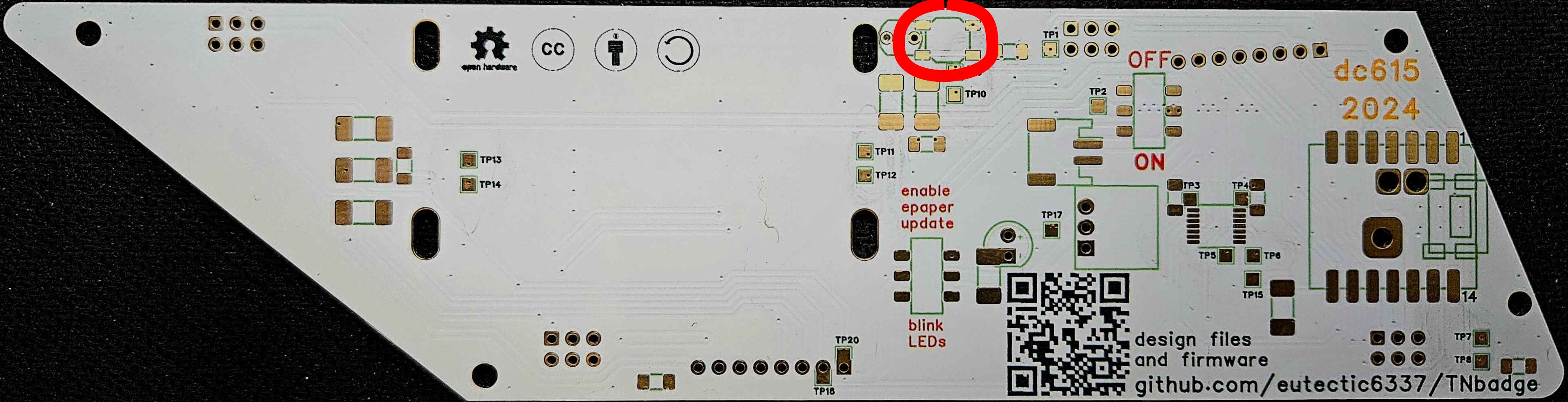
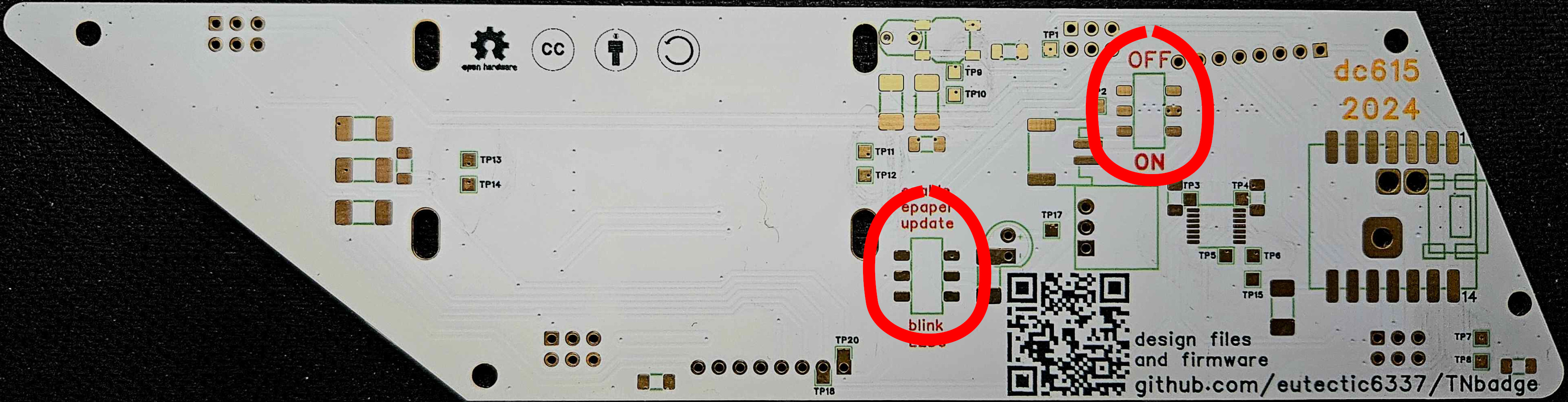


4 layers40 × 40 mm
Raspberry pi IMX662
BellssGit/IMX662_module_for_raspberry_pi
A simple camera module for Raspberry Pi using IMX662 sensor
48 parts12GPL-2.0

Data point: after soldering only the front components (5x smart LED, 2x resistor) on 5 boards, I had 1 board with no erroneous beeps in the continuity test.
Badge is an open-source printed circuit board by eutectic6337, from the eutectic6337/TNbadge repository on GitHub. It is a 2-layer board of 190.9 × 48.3 mm with 69 parts on 44 nets, routed with 602 tracks and 138 vias.
It is built around the TXS0104EPWR-TP. Its parts include 10 resistors, 7 capacitors, 6 diodes, 5 ICs and 4 connectors. It belongs with the lEDs and displays boards and the ESP32 and RISC-V boards of this library.
designed in Kicad
imported into EasyEDA Pro
manually reattached lanyard/stencil-alignment holes, battery box slots, an zero-size holes to net GND with direct connect (i.e. no thermal relief)
manually reattached quarter-circle track around pin 2 of epaper display connector, top left, to net /GPIO1{SLASH}DC
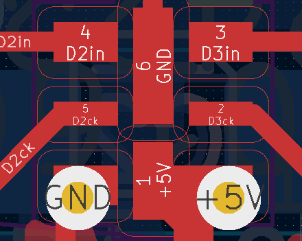
manually re-edited APA102 footprint to remove solder mask/stencil openings over (center) duplicate GND/5V pads
manually edited all testpoints to show correct designator, on back silkscreen layer
manually imported QR code PNG (M1) onto back silkscreen layer (Kicad plays poorly)
manually adjusted color of silkscreen artifacts
multicolour PNG artwork imported to front silkscreen layer
ordered from JLC PCB
already in hand (through-hole LDRs)
LCSC (SMD resistors & capacitors)
Seeed Studio (CPU module)
AliExpress (everything else)
position PCB back-down on stable heat-resistant surface
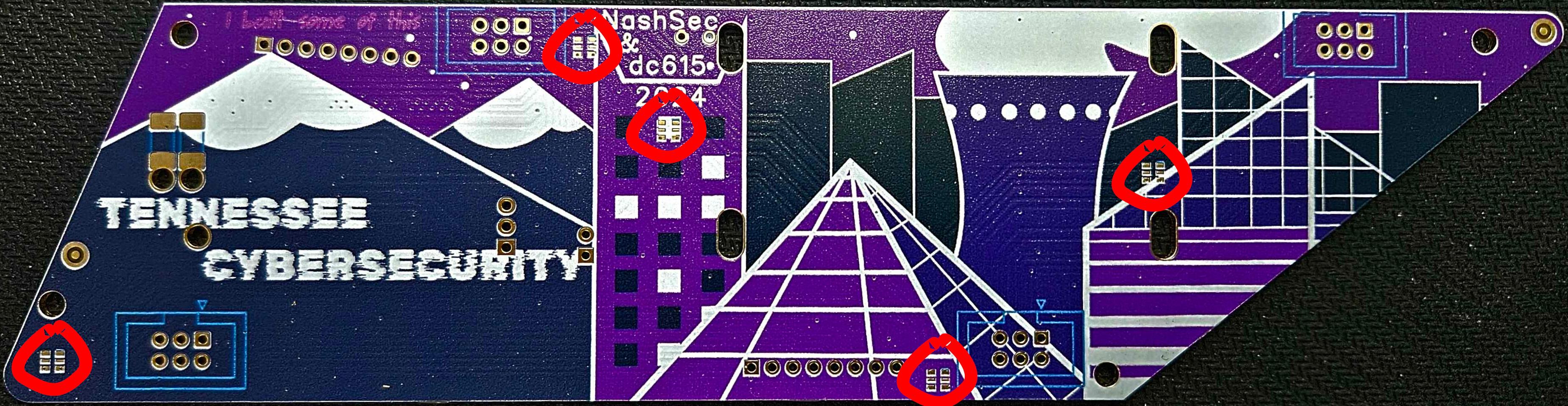
stencil solder paste on front
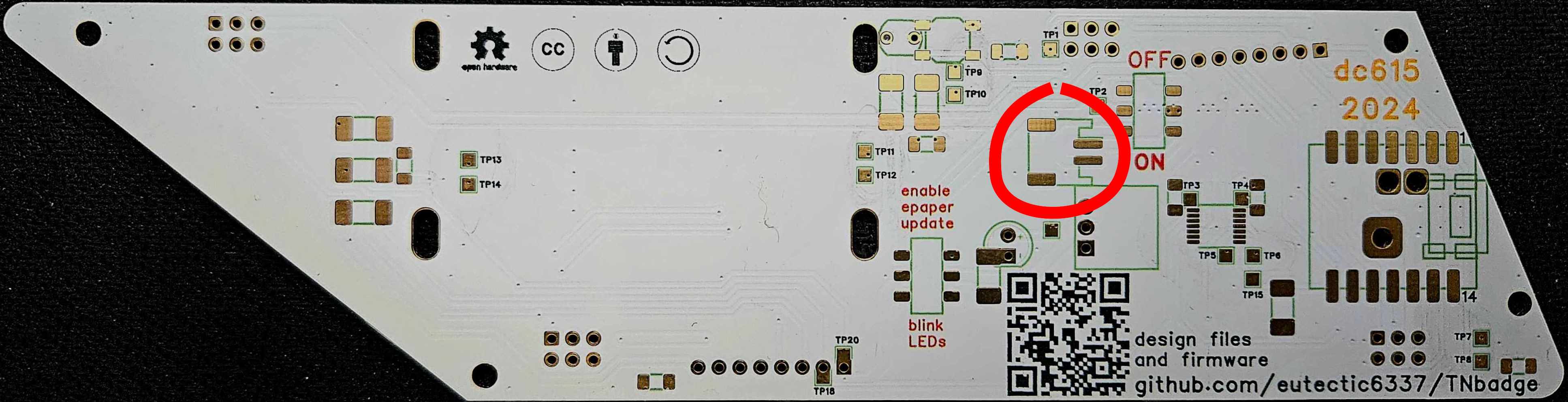
place 2x 100k resistor (2010)
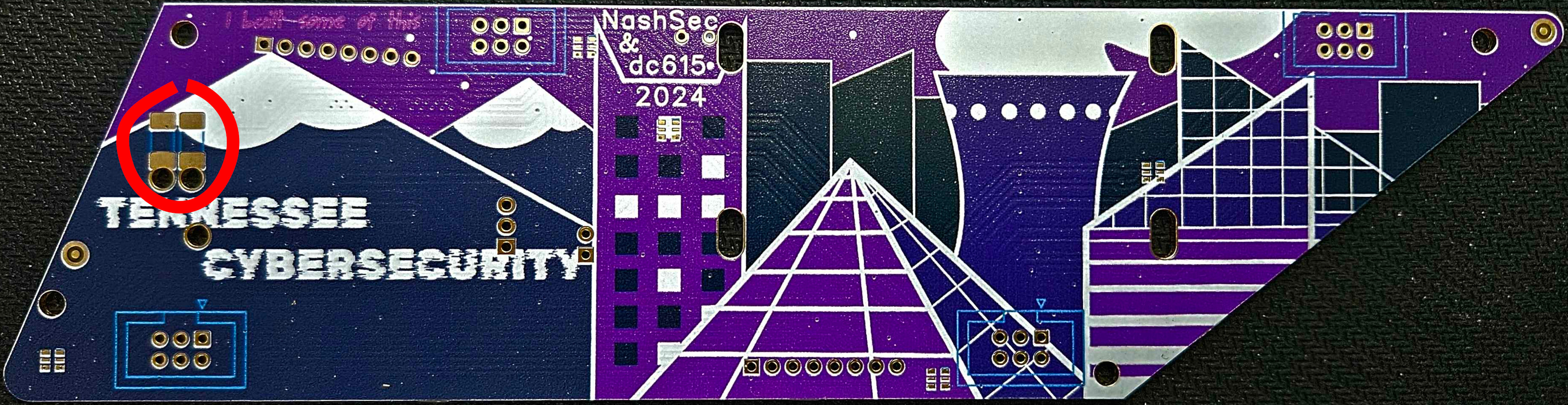
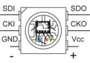
place 5x APA102 addressable RGB LED (2020)
(optional) preheat to 100 degC
apply hot air at 200+ degC to each component until solder flows to create concave surface
position board front-down on stable non-conductive surface
starting at lower right corner, test continuity between each pair of pads from the set {test points, CPU pads}
continuity is expected between
TP1 CPU13 CPU_GND CPU_BAT-
TP2 CPU_BAT+
TP3 CPU12
TP15 CPU8
TP18 CPU7
TP20 CPU1
continuity between any pair of test points, or between any pair of CPU pads, or between any other test points and CPU pads indicates a likely solder bridge
continuity between any of TP5 through TP14 and TP4 or TP1 indicates a bridge between pads of one of the smart LEDs either side of the involved TP5...TP14
Data point: after soldering only the front components (5x smart LED, 2x resistor) on 5 boards, I had 1 board with no erroneous beeps in the continuity test.
For each identified fault
desolder identified likely culprit components
flux and wick up solder from PCB
re-test to verify fault is gone; if fault remains, dig deeper
flux pads and reposition component
reflow remaining solder
add minimal solder if needed
re-test to verify fault is gone
Mr Clumsyhands has found a trap for young players: once you've played some hot air over a SMD LED, its little transparent top becomes soft enough for your tweezers to wipe it off, along with the actual silicon bits underneath, if you twitch while applying pressure to the side of the package.
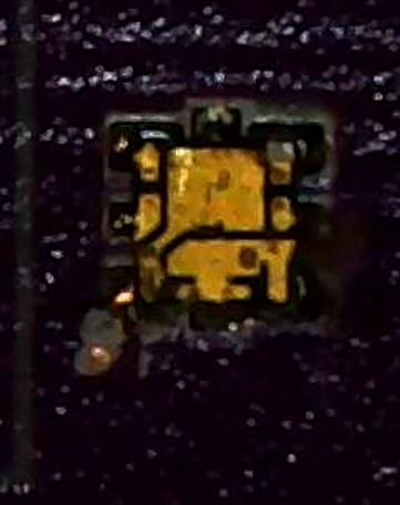
So, don't do that.
position PCB front-down on stable heat-resistant surface
stencil solder paste on back
place 1x level shifter chip (TSSOP)
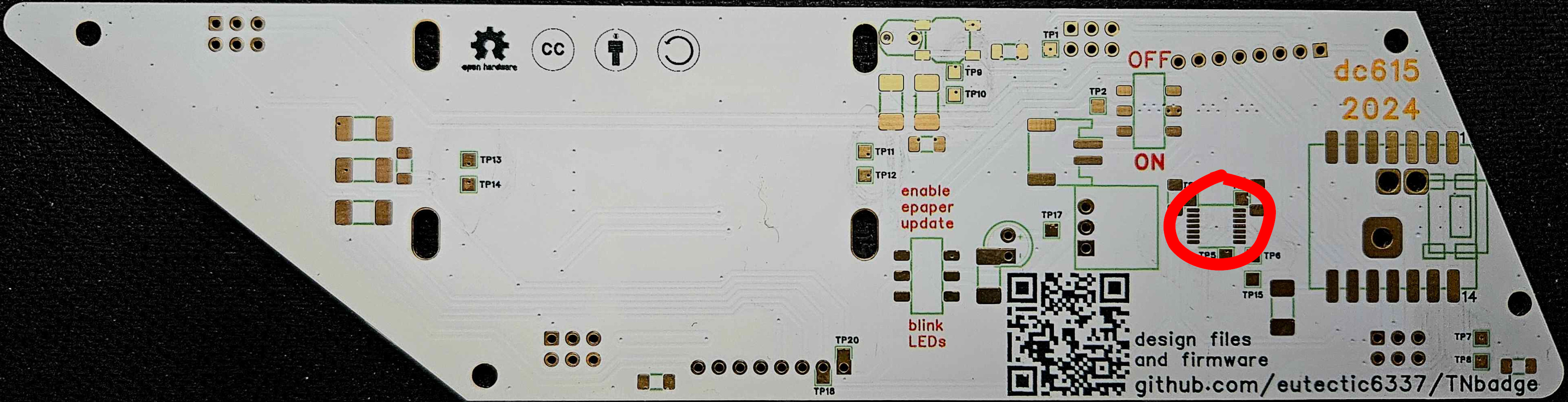
place 1x 100 ohm resistor (2010)
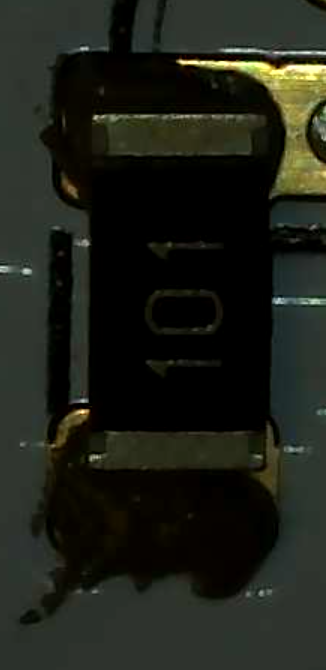
place 6x 10k resistor (2010)
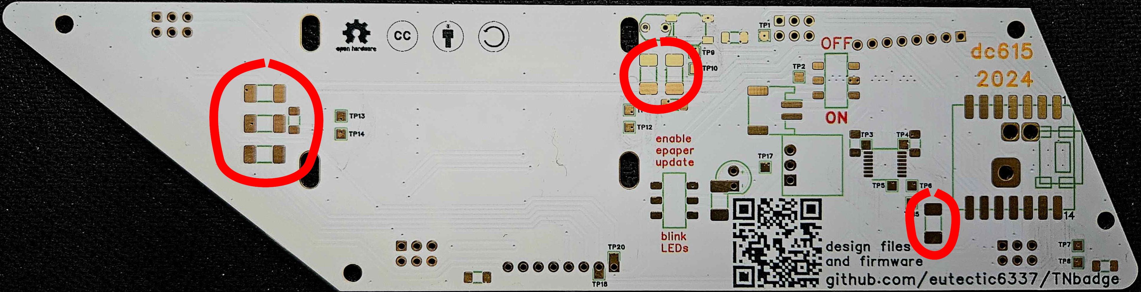
place 7x 1uF capacitor (1206)
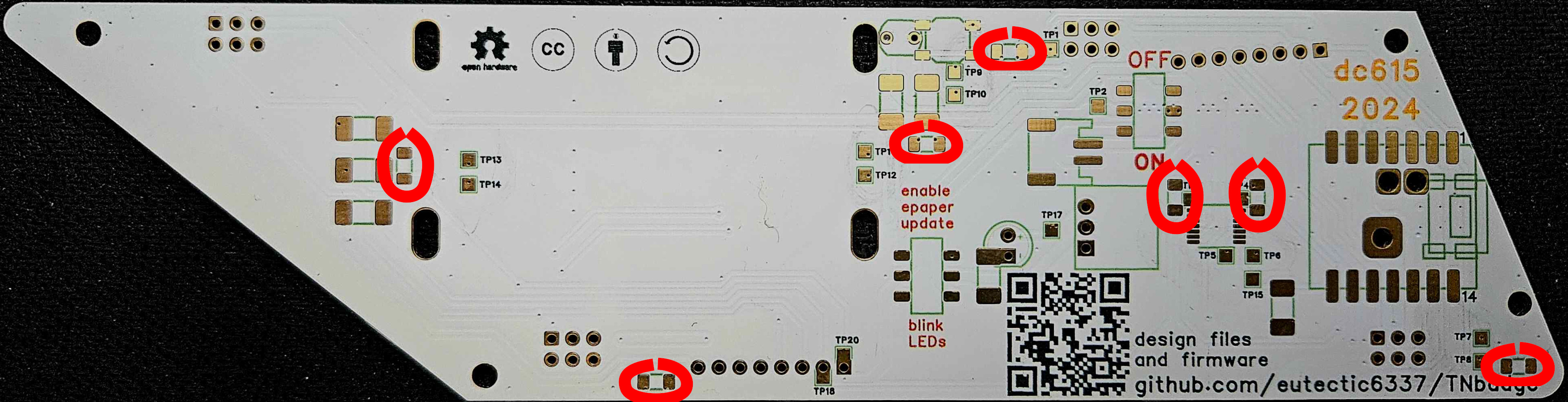
(optional) preheat to 100 degC
apply hot air at 200+ degC to each component until solder flows to create concave surface
position board front-down on stable non-conductive surface
starting at lower right corner, test continuity between each pair of pads from the set {test points, CPU pads}
continuity is expected between
TP1 CPU13 CPU_GND CPU_BAT-
TP2 CPU_BAT+
TP3 CPU12
TP15 CPU8
TP18 CPU7
TP20 CPU1
continuity between any pair of test points, or between any pair of CPU pads, or between any other test points and CPU pads indicates a likely solder bridge
most likely location for bridge is TSSOP level shifter chip
flux and wick up excess solder from pins on one side
drag-solder with small wedge/chisel tip iron to reflow remaining solder
re-test to verify fault is gone; if fault remains, dig deeper
For each other identified fault
desolder identified likely culprit components
flux and wick up solder from PCB
re-test to verify fault is gone; if fault remains, dig deeper
flux pads and reposition component
reflow remaining solder
add minimal solder if needed
re-test to verify fault is gone
position PCB front-down on stable heat-resistant surface
apply small dot of solder paste on each of 14 main CPU pads on PCB
place ESP32C3 CPU module
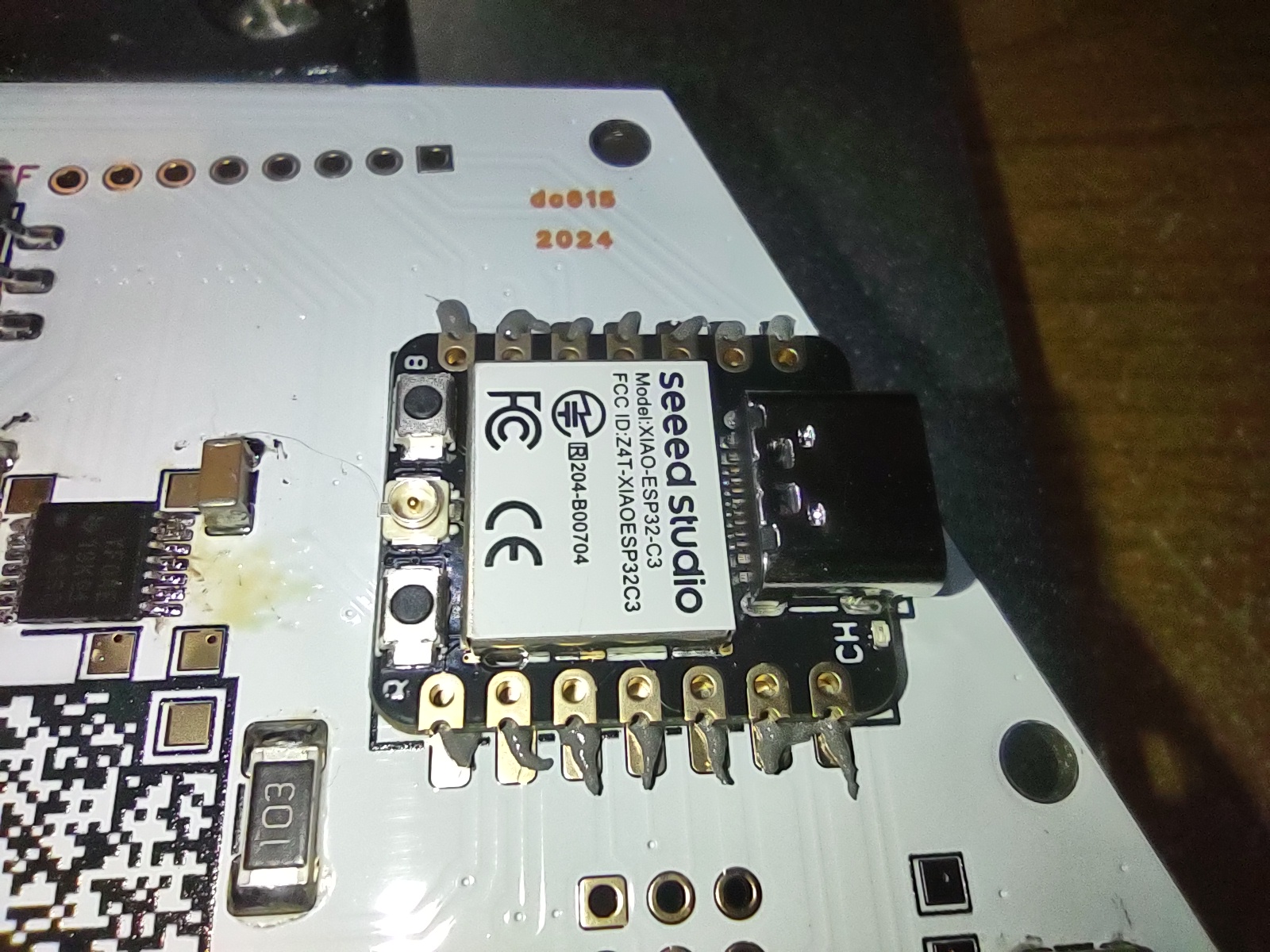
apply hot air at 200+ degC to each long edge of CPU carrier board
until solder flows to create concave surface
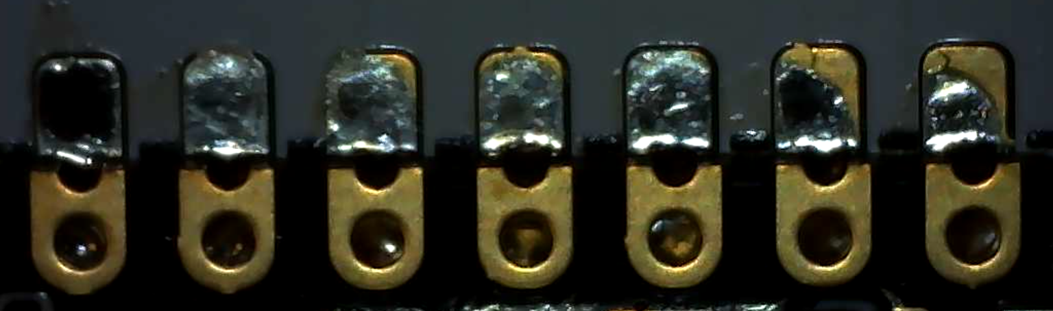
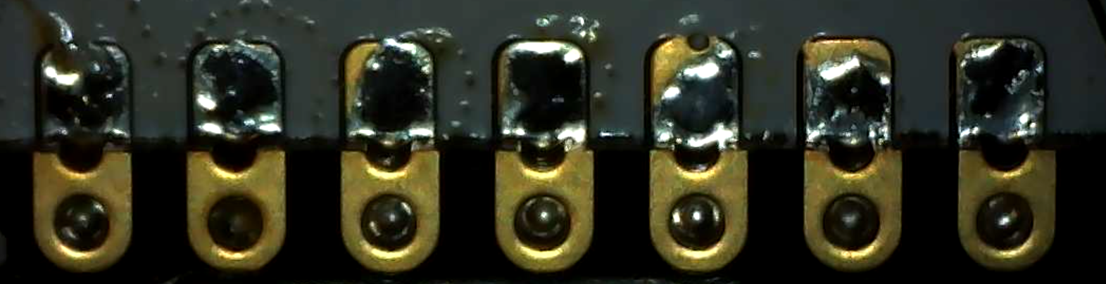
position PCB back-down on stable heat-resistant surface
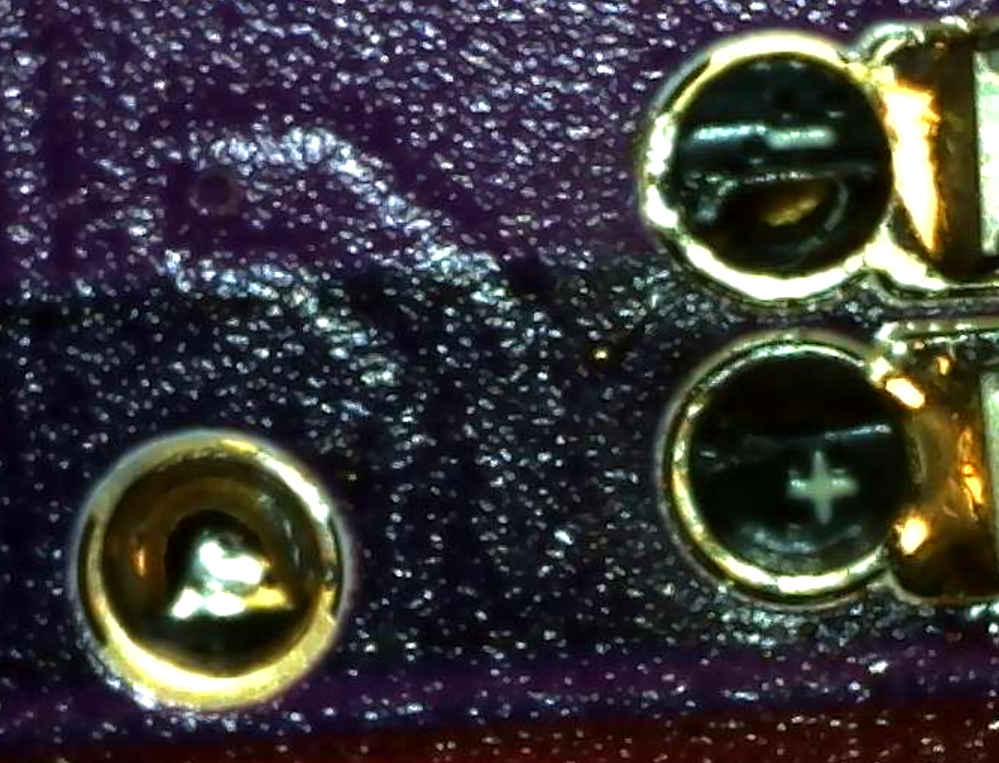
apply small dot of solder paste in each of 3 through-holes under CPU module
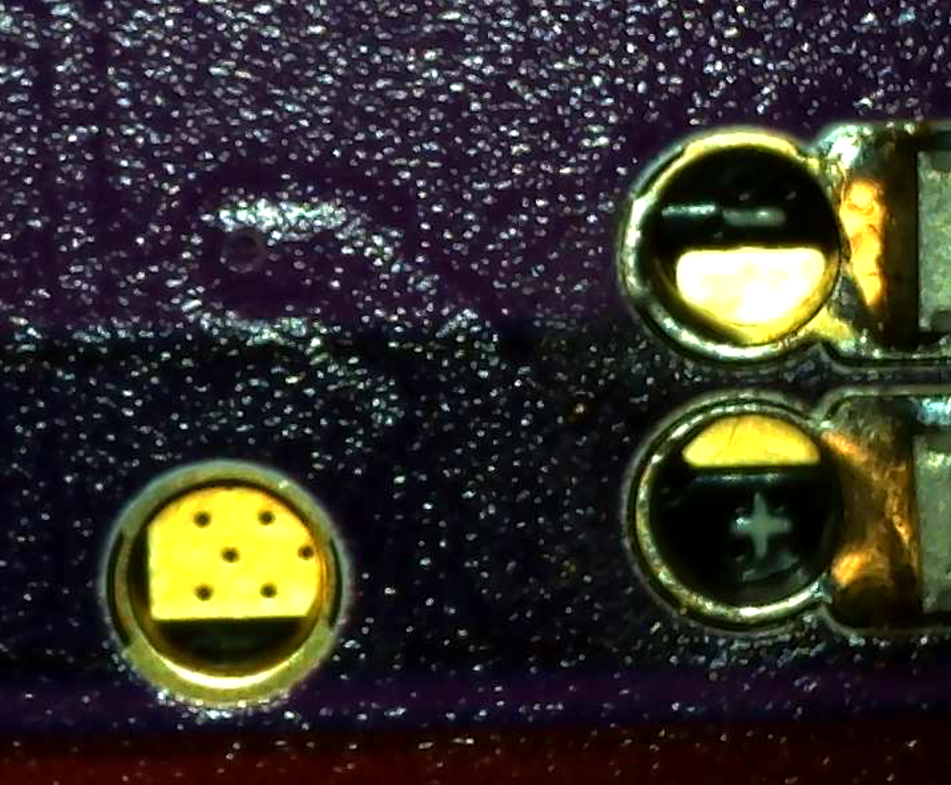
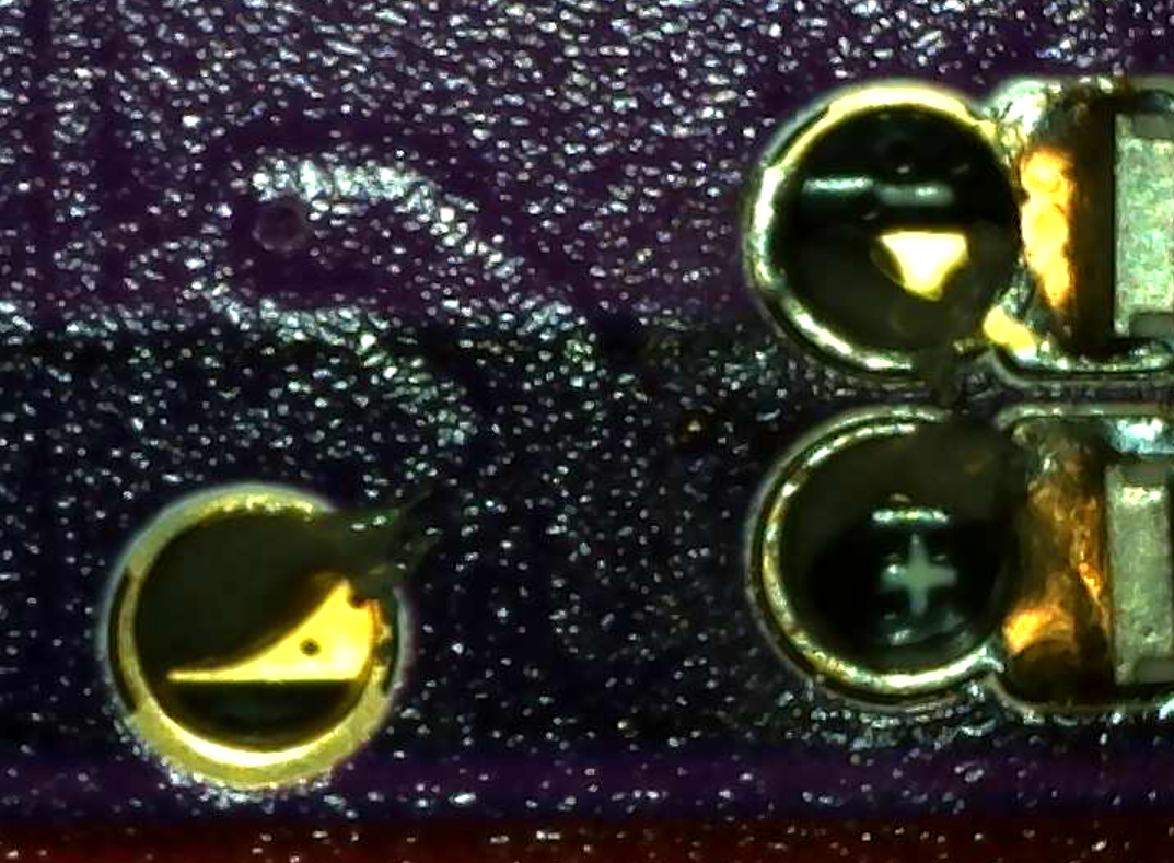
apply hot air at 200+ degC to holes under CPU carrier board
until solder flows to create concave surface
| Qty | Value | Footprint | References |
|---|---|---|---|
| 7 | 1u | Capacitor_SMD:C_1206_3216Metric_Pad1.33x1.80mm_HandSolder | C1, C2, C3, C4, C5, C41, C42 |
| 6 | 10k | Resistor_SMD:R_2010_5025Metric_Pad1.40x2.65mm_HandSolder | R1, R3, R4, R5, R7, R41 |
| 5 | APA102 | extra:LED-APA102-2020 | D1, D2, D3, D4, D5 |
| 4 | MountingHole_2.2mm_M2_DIN965_Pad | MountingHole:MountingHole_2.2mm_M2_DIN965_Pad | bb1, bb2, bb5, bb6 |
| 4 | SAO V.1.69bis host | Connector_IDC:IDC-Header_2x03_P2.54mm_Vertical | J1, J1, J1, J1 |
| 2 | lanyard1, lanyard2 | ||
| 2 | 100k | Resistor_SMD:R_2010_5025Metric_Pad1.40x2.65mm_HandSolder | R9, R10 |
| 2 | Fiducial_1mm_Mask3mm | Fiducial:Fiducial_1mm_Mask3mm | fiducial1, fiducial2 |
| 2 | MH-ET_epaper_ 2.13 | extra:MH-ET_epaper_ 2.13 | U2, U2 |
| 1 | /RST | TestPoint:TestPoint_Pad_1.5x1.5mm | TP18 |
| 1 | 0V | TestPoint:TestPoint_Pad_1.5x1.5mm | TP1 |
| 1 | 100 | Resistor_SMD:R_2010_5025Metric_Pad1.40x2.65mm_HandSolder | R11 |
| 1 | 3.3V | TestPoint:TestPoint_Pad_1.5x1.5mm | TP3 |
| 1 | 4.1V | TestPoint:TestPoint_Pad_1.5x1.5mm | TP2 |
| 1 | 5V | TestPoint:TestPoint_Pad_1.5x1.5mm | TP4 |
| 1 | 5V boost converter | extra:boost converter module | U3 |
| 1 | BUSY | TestPoint:TestPoint_Pad_1.5x1.5mm | TP20 |
| 1 | Battery | Connector_JST:JST_PH_S2B-PH-SM4-TB_1x02-1MP_P2.00mm_Horizontal | BT1 |
| 1 | D1clk | TestPoint:TestPoint_Pad_1.5x1.5mm | TP6 |
| 1 | D1in | TestPoint:TestPoint_Pad_1.5x1.5mm | TP5 |
| 1 | D2clk | TestPoint:TestPoint_Pad_1.5x1.5mm | TP8 |
| 1 | D2in | TestPoint:TestPoint_Pad_1.5x1.5mm | TP7 |
| 1 | D3clk | TestPoint:TestPoint_Pad_1.5x1.5mm | TP10 |
| 1 | D3in | TestPoint:TestPoint_Pad_1.5x1.5mm | TP9 |
| 1 | D4clk | TestPoint:TestPoint_Pad_1.5x1.5mm | TP12 |
| 1 | D4in | TestPoint:TestPoint_Pad_1.5x1.5mm | TP11 |
| 1 | D5clk | TestPoint:TestPoint_Pad_1.5x1.5mm | TP14 |
| 1 | D5in | TestPoint:TestPoint_Pad_1.5x1.5mm | TP13 |
| 1 | LDR07 | OptoDevice:R_LDR_5.1x4.3mm_P3.4mm_Vertical | R2 |
| 1 | LED | LED_THT:LED_D5.0mm | D6 |
| 1 | LEDin | TestPoint:TestPoint_Pad_1.5x1.5mm | TP17 |
| 1 | OE | TestPoint:TestPoint_Pad_1.5x1.5mm | TP15 |
| 1 | OSHW-Logo2_7.3x6mm_SilkScreen | Symbol:OSHW-Logo2_7.3x6mm_SilkScreen | OSHW |
| 1 | SW_Push | Button_Switch_SMD:SW_SPST_SKQG_WithoutStem | SW2 |
| 1 | Seeed XIAO ESP32-C3 | extra:Seeed XIAO ESP32-C3 hand-solderable | U1 |
| 1 | Symbol_CC-Attribution_Silkscreen_Small | extra:Symbol_CC-Attribution_Silkscreen_Small | CC-BY |
| 1 | Symbol_CC-ShareAlike_Silkscreen_Small | extra:Symbol_CC-ShareAlike_Silkscreen_Small | CC-SA |
| 1 | Symbol_CreativeCommons_Silkscreen_Type2_Small | extra:Symbol_CreativeCommons_Silkscreen_Type2_Small | CC |
| 1 | TXS0104EPWR | Package_SO:TSSOP-14_4.4x5mm_P0.65mm | U4 |
| 1 | power | extra:MSS-22D18G2 hand-solderable | SW1 |
| 1 | update epaper | extra:MSS-22D18G2 hand-solderable | SW3 |
The 66 most common of 69 parts.
It measures 190.9 × 48.3 mm and has 2 copper layers, 1.6 mm thick.
69 parts, built around the TXS0104EPWR-TP. The full list of its parts is on this page, with links to each part's symbol and footprint where PCBKit's library has them.
From the eutectic6337/TNbadge repository on GitHub, at the commit this page was made from: the board is hardware/badge.kicad_pcb and its schematic hardware/badge.kicad_sch. PCBKit opens the board in the browser, with nothing to install.
Its repository states no licence, so its author keeps all rights: ask eutectic6337 before reusing the design.
BellssGit/IMX662_module_for_raspberry_pi
A simple camera module for Raspberry Pi using IMX662 sensor

Case-Rocket-Team/PayloadPrototypeBoard2021
Prototype Payload Board for the 2021 ESRA Payload using Parafoil Guidance. KiCad Project


pebender/wireless_adapter_for_mitsubishi
This project is neither associated with nor endorsed by Mitsubishi Electric. By using this project, you may void your warranty or break your heat pump.


hackclub/OnBoard
💡 Join 1,000 teenagers and make your first PCB with a $100 grant!

K-0hm/Chessboard
Code for a chessboard with light and capacitance Touch Sensors.