4 layers50 × 80 mm
ARGOS DEMO
CNES/argos-demo-board
Demo board designed to use the ARRIBADA SMD module via USB to send ARGOS messages to the Kineis constellation.
91 parts7CERN-OHL-S-2.0
 Ethan-Scanlon/dataBoardTransfer1
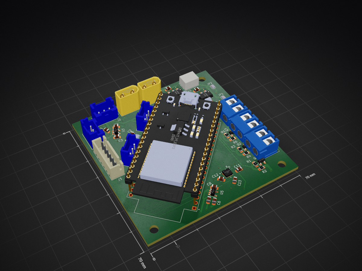
IO:Sensor Board is an open-source printed circuit board by Ethan-Scanlon, from the Ethan-Scanlon/dataBoardTransfer repository on GitHub. It is a 4-layer board of 70 × 70 mm with 46 parts on 67 nets, routed with 341 tracks and 40 vias.
It is built around the BMP581, XT30UPB-M and ICM-20948, with the B3B-XH-A, DMN3023L-7 and B2B-XH-A among its other parts. Its parts include 15 capacitors, 9 ICs, 9 connectors, 6 resistors and 3 transistors. It belongs with the sensors and measurement boards and the ESP32 boards of this library.


| Qty | Value | Footprint | References |
|---|---|---|---|
| 9 | 0.1uF | Capacitors:C_0805_2012Metric_Pad1.18x1.45mm_HandSolder | C1, C2, C3, C4, C5, C6, C11, C12, C13 |
| 4 | 10uF | Capacitors:C_0805_2012Metric_Pad1.18x1.45mm_HandSolder | C7, C8, C10, C14 |
| 3 | 1k | Resistor:R_0805_2012Metric_Pad1.20x1.40mm_HandSolder | R1, R3, R5 |
| 3 | 282837-2 | ScrewTerminal:CUI_TB002-500-02BE | P1, P2, P3 |
| 3 | 470 | Resistor:R_0805_2012Metric_Pad1.20x1.40mm_HandSolder | R2, R4, R6 |
| 3 | B3B-XH-A | B3B:CONN_B3B-XH-A_JST | J1, J2, J5 |
| 3 | DMN3023L-7 | FETS:SOT96P240X100-3N | Q1, Q2, Q3 |
| 3 | Jumper_2_Open | Jumper:SolderJumper-2_P1.3mm_Open_RoundedPad1.0x1.5mm | JP1, JP2, JP3 |
| 2 | 100uF | Capacitors:C_0805_2012Metric_Pad1.18x1.45mm_HandSolder | C9, C15 |
| 2 | LD1117S50CTR | LD1117S50CTRlib:LD1117S50CTR | U7, U9 |
| 2 | XT30UPB-M | XTConnectors:XT30UPB-M | U8, U10 |
| 1 | B2B-XH-A | B2B-XH-A:CONN_B2B-XH-A_JST | J4 |
| 1 | B3B-XH-A | NewJST:CONN_B3B-XH-A_JST | J6 |
| 1 | B6B-XH-A | Connector_JST:JST_XH_B6B-XH-A_1x06_P2.50mm_Vertical | J3 |
| 1 | BMP581 | footprints:QFN10_BMP581_BOS | U1 |
| 1 | DEVKIT_V1_ESP32-WROOM-32 | esp32wroom:MODULE_DEVKIT_V1_ESP32-WROOM-32 | U2 |
| 1 | ICM-20948 | ICM-20948:QFN24_3X3X0P9_IVS | U4 |
| 1 | LOGO | GRPImages:GRPLogo | G*** |
| 1 | TPS79318-EP | Package_TO_SOT_SMD:SOT-23-5 | U5 |
| 1 | TPS79333-EP | Package_TO_SOT_SMD:SOT-23-5 | U3 |
It measures 70 × 70 mm and has 4 copper layers, 1.6 mm thick.
46 parts, built around the BMP581, XT30UPB-M, ICM-20948 and B3B-XH-A. The full list of its parts is on this page, with links to each part's symbol and footprint where PCBKit's library has them.
From the Ethan-Scanlon/dataBoardTransfer repository on GitHub, at the commit this page was made from: the board is GRPv1.2RasToNew/IO:Sensor Board.kicad_pcb and its schematic GRPv1.2/GRPv1.2.kicad_sch. PCBKit opens the board in the browser, with nothing to install.
Its repository states no licence, so its author keeps all rights: ask Ethan-Scanlon before reusing the design.
CNES/argos-demo-board
Demo board designed to use the ARRIBADA SMD module via USB to send ARGOS messages to the Kineis constellation.

themarcolab/Stardrive-Shield
With STARDRIVE SHIELD you can implement from 6 step to FOC motor control algorithms.

kylenmorris/reaction-chamber
A custom reaction chamber for automation of crop pathogens testing using a NAAT reaction, developed as a capstone project

gustebeast/public-steel-guitar
A pedal steel guitar you can build yourself, from parts anyone can buy.


nischayhegde/jetson_spi_to_can_x8_breakout
A PCB board for expanding the SPI channels on Jetson Orin nano super into 8 CANfd channels. Comes with chip select logic and jetpack drivers. Supports 1Mbit per CAN channel.

