2 layers46 × 19 mm
MCU Link Standalone
ErichStyger/McuLink-Mini
Version of the NXP MCU-Link Debug CMSIS-DAP Debug Probe.
69 parts32MIT

 ErichStyger/MCU-Link-MR20
Open Source MCU-Link CMSIS-DAP Debug probe for mobile robots (e.g. Pixhawk)
MCU Link MR is an open-source printed circuit board by ErichStyger, from the ErichStyger/MCU-Link-MR repository on GitHub, published under the MIT licence. It is a 2-layer board of 57.9 × 39.9 mm with 121 parts on 87 nets, routed with 1,351 tracks and 319 vias.
It is built around the MCP6001T-I/OT(MS), 74LVC1T45GW and 74LVC2T45DC, with the LPC55S69JBD64, XC6227C331PR-G and MPZ1608S331ATD25 among its other parts. Its parts include 47 capacitors, 28 resistors, 11 ICs, 9 connectors and 7 inductors. It belongs with the robots and motor control and sensors and measurement boards and the NXP (LPC, Kinetis, i.MX RT) boards of this library.


Project for the NXP MCU-Link Debug Probe with KiCAD, as a debug drone for mobile robotics platforms.
This project is hosted on GitHub: https://github.com/ErichStyger/MCU-Link-MR
See https://mcuoneclipse.com/2024/05/05/cmsis-dap-debug-probe-for-robots-and-pixhawk-with-kicad/
You can order the v0.2 board as produced by NXP: https://www.nxp.com/design/design-center/software/development-software/mcuxpresso-software-and-tools-/mcu-link-mr-debug-probe-with-usb-c-serial-and-mobile-robotics-interfaces:MCU-LINK-MR. See the package content and getting started at https://mcuoneclipse.com/2025/04/13/mcu-link-mr-affordable-cmsis-dap-debug-probe-for-robotics-and-beyond/
The MCU-Link-MR is an open source debug probe, based on the original NXP MCU-Link.
The MCU-Link-MR supports debugging ARM-Cortex devices plus includes multiple headers used for robots and drone projects.
Renderings below show the v0.2 version.
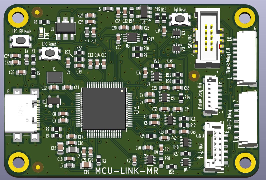
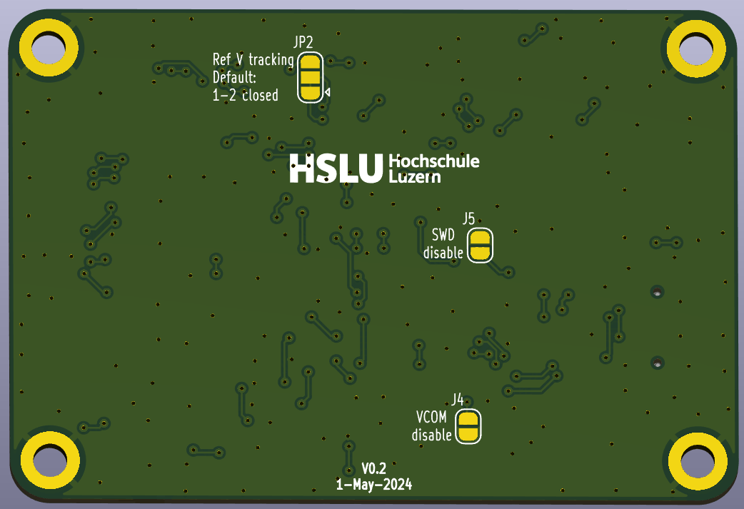
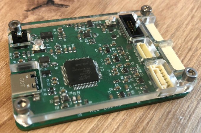
The first v0.1 version and the v0.2 version:
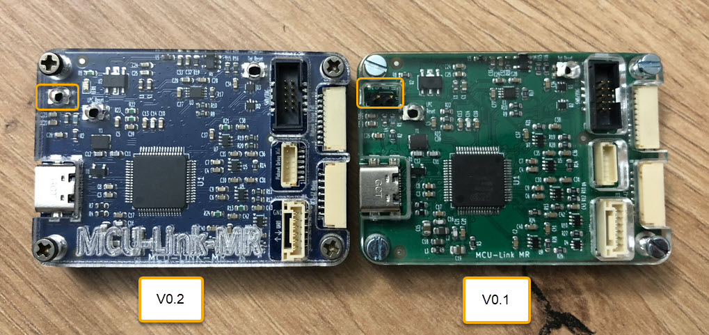
PCB of the v0.2:
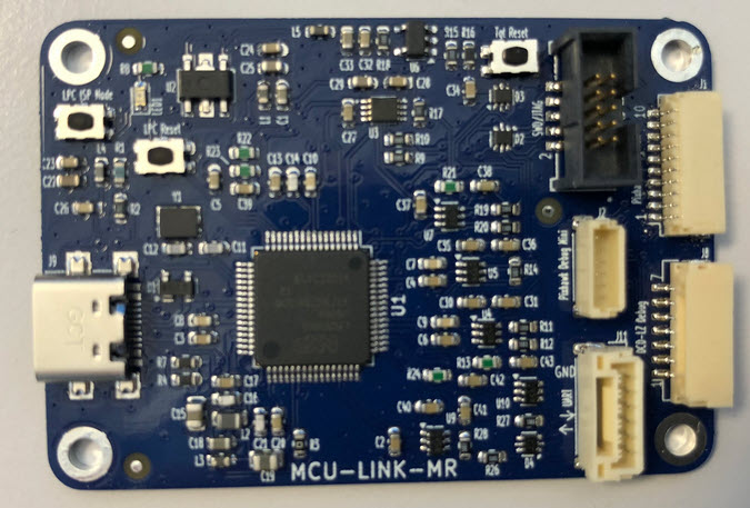
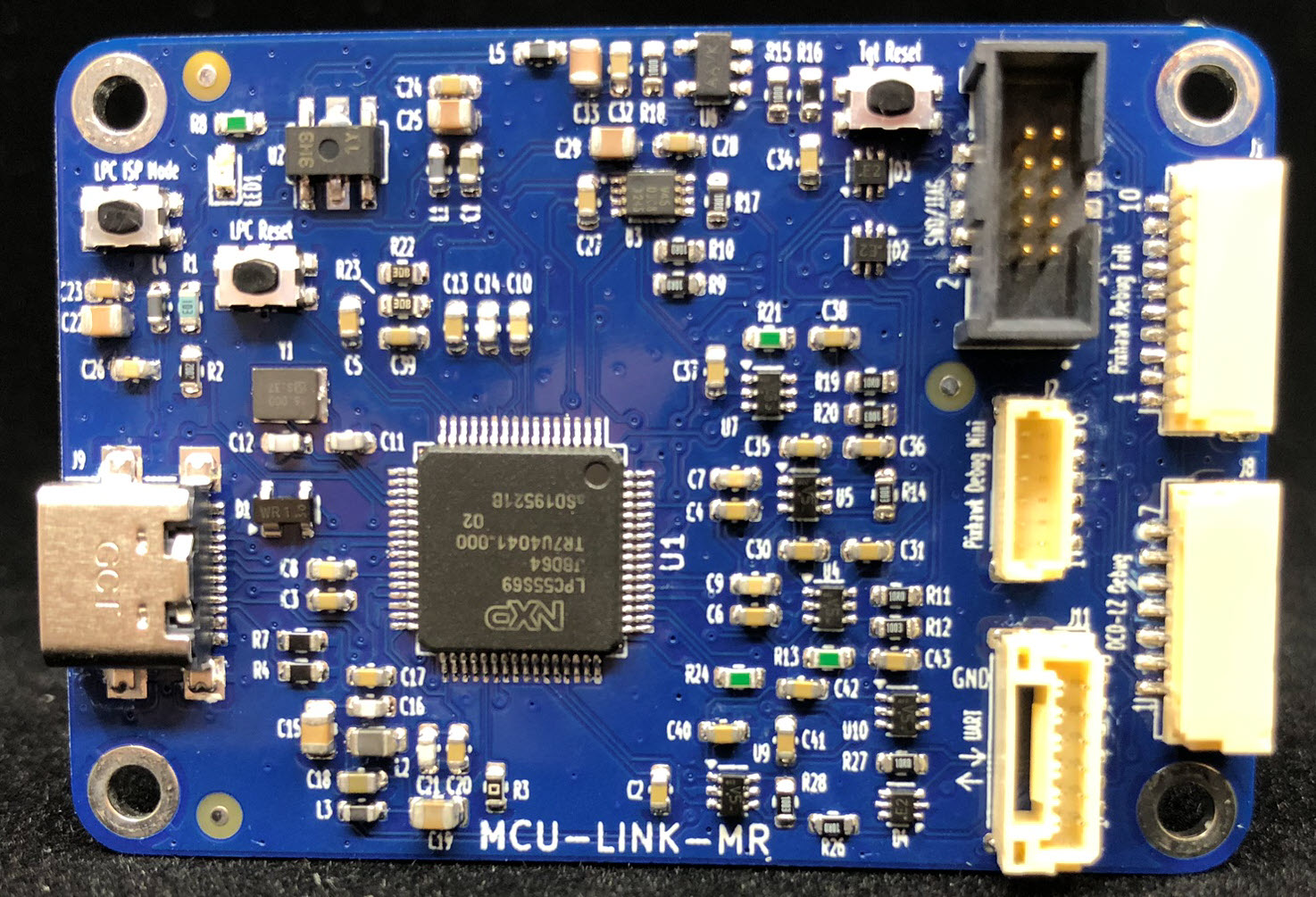
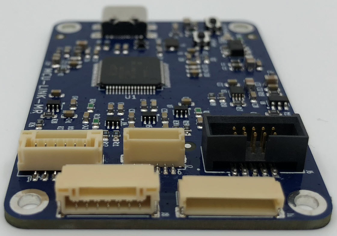
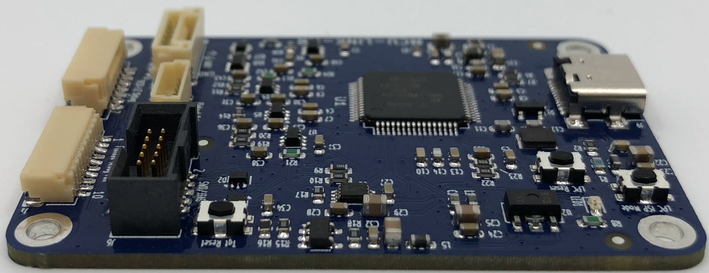
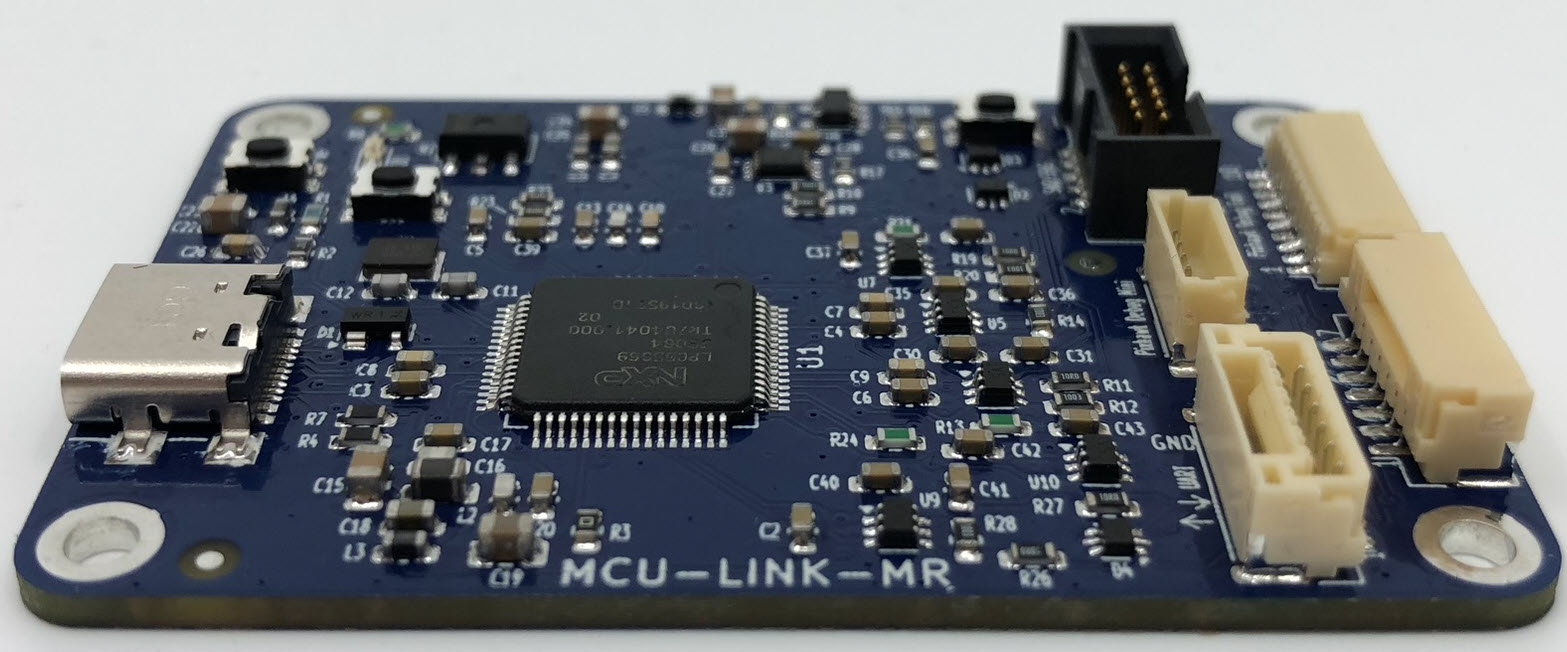
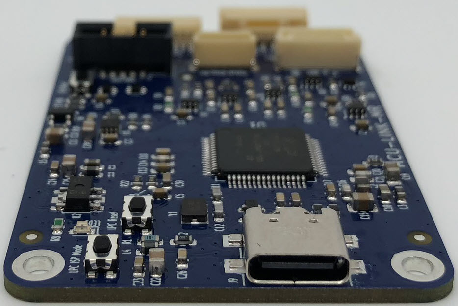
PCB of the v0.3:
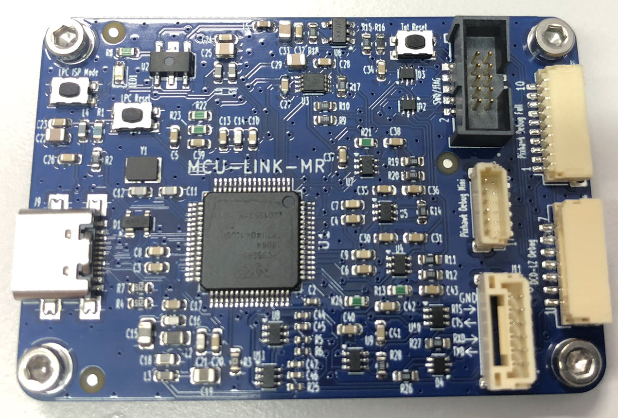
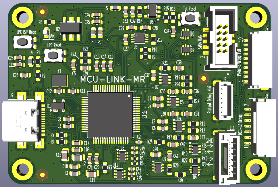
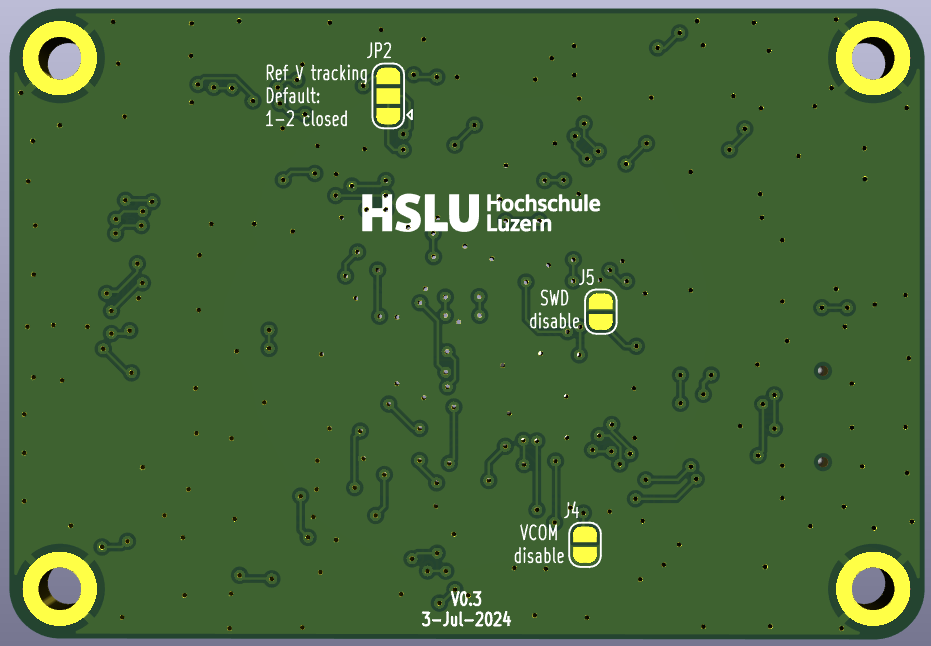
PCB of the v0.4:
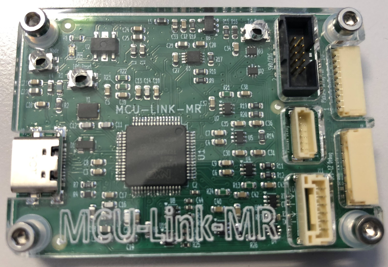
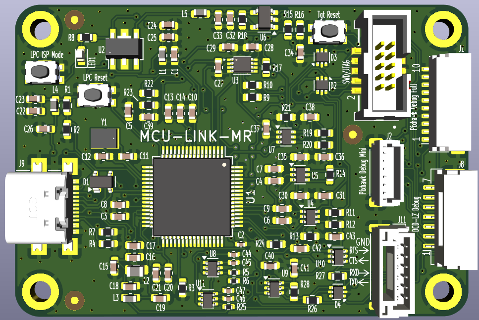
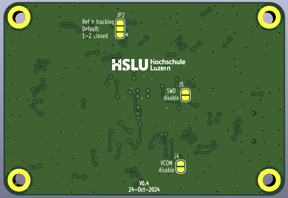
PCB of the v0.5:
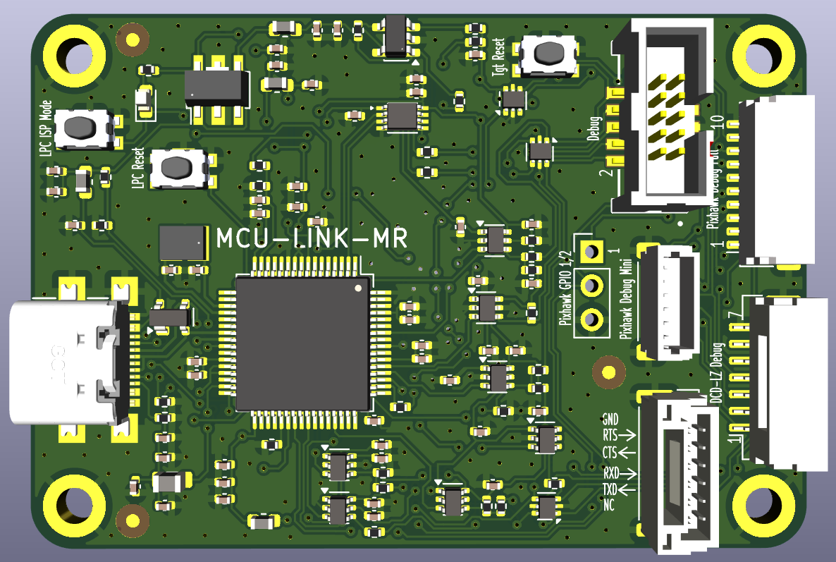
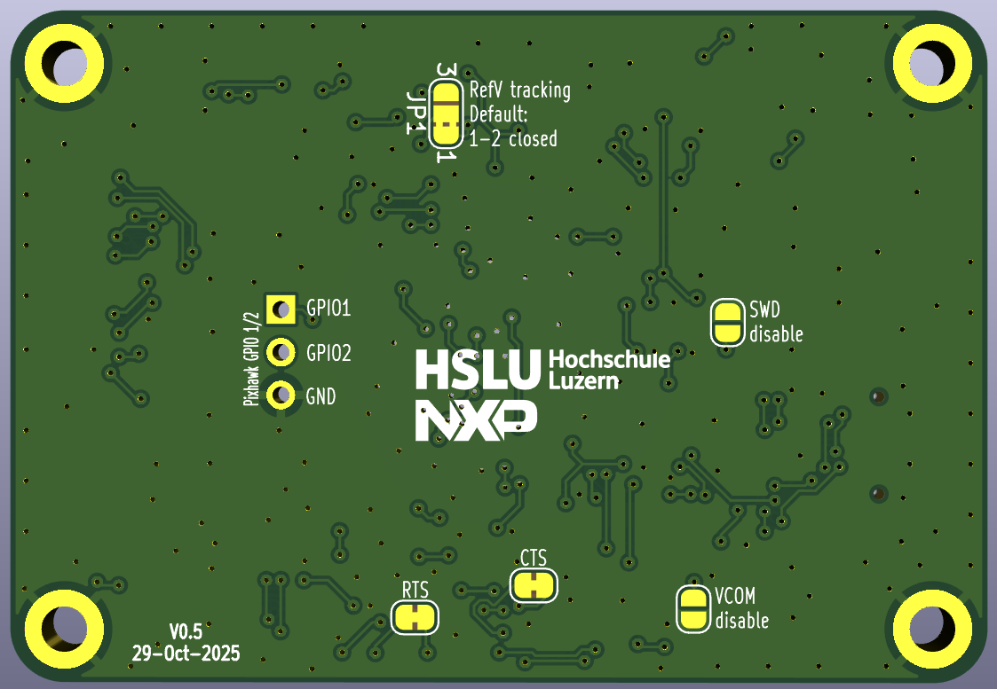
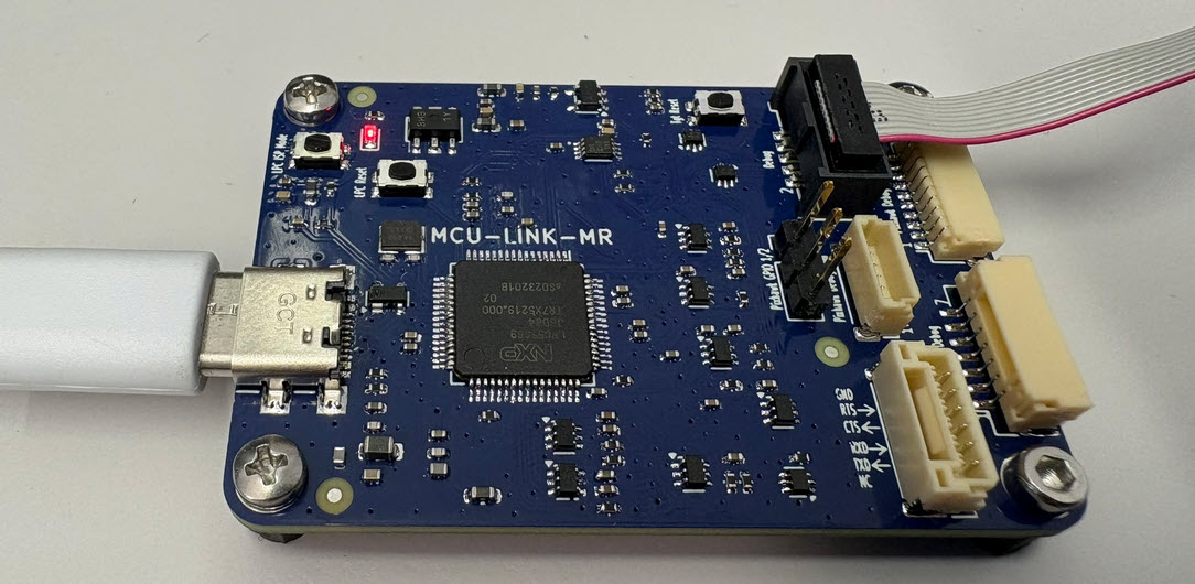
The gerber files for the different releases can be found in KiCAD project directory.
PCBs have been produced by PCBWay (https://www.pcbway.com/), with following settings:
| Qty | Value | Footprint | References |
|---|---|---|---|
| 29 | 100nF 6.3V | Capacitor_SMD:C_0402_1005Metric | C2, C3, C13, C17, C20, C23, C24, C27, C28, C30, C31, C32, C34, C35, C36, C37 +13 |
| 9 | 10R 5% 100mW | Resistor_SMD:R_0402_1005Metric | R6, R9, R10, R11, R17, R19, R25, R26, R27 |
| 7 | 74LVC1T45GW | Package_TO_SOT_SMD:SOT-363_SC-70-6 | U4, U5, U7, U8, U9, U10, U11 |
| 6 | 2k 5% 100mW | Resistor_SMD:R_0402_1005Metric | R8, R13, R21, R22, R23, R24 |
| 5 | 100k 5% 100mW | Resistor_SMD:R_0402_1005Metric | R5, R12, R14, R20, R28 |
| 5 | 10nF 6.3V | Capacitor_SMD:C_0402_1005Metric | C7, C8, C9, C10, C26 |
| 4 | 10uF 6.3V | Capacitor_SMD:C_0402_1005Metric | C22, C25, C29, C33 |
| 4 | MPZ1608S331ATD25 | Inductor_SMD:L_0603_1608Metric | L1, L3, L4, L5 |
| 4 | MountingHole_Pad | MountingHole:MountingHole_2.7mm_M2.5_DIN965_Pad | H1, H2, H3, H4 |
| 3 | 22uF 6.3V | Capacitor_SMD:C_0402_1005Metric | C15, C18, C19 |
| 3 | 47pF 6.3V | Capacitor_SMD:C_0402_1005Metric | C14, C16, C21 |
| 3 | Fiducial | McuOnEclipse:Fiducial_1mm_Dia_2.54mm_Outer_CopperTop | FID1, FID2, FID3 |
| 3 | KMR221GLFS | McuOnEclipse:SW_C_K_KMR2 | SW1, SW2, SW3 |
| 3 | PESD5V0L5UV,115 | Package_TO_SOT_SMD:SOT-666 | D2, D3, D4 |
| 2 | 100R 5% 100mW | Resistor_SMD:R_0402_1005Metric | R15, R18 |
| 2 | 5.1k 5% 100mW | Resistor_SMD:R_0402_1005Metric | R4, R7 |
| 2 | 8pF 6.3V | Capacitor_SMD:C_0402_1005Metric | C11, C12 |
| 2 | Jumper_2_Open | McuOnEclipse:SolderJumper-2_P1.3mm_Open_RoundedPad1.0x1.5mm | J4, J5 |
| 1 | 0R 5% 100mW | Resistor_SMD:R_0402_1005Metric | R3 |
| 1 | 10k 5% 100mW | Resistor_SMD:R_0402_1005Metric | R1 |
| 1 | 20k 5% 100mW | Resistor_SMD:R_0402_1005Metric | R2 |
| 1 | 33k 5% 100mW | Resistor_SMD:R_0402_1005Metric | R16 |
| 1 | 4.6uH | Inductor_SMD:L_0805_2012Metric | L2 |
| 1 | 4.7uF 6.3V | Capacitor_SMD:C_0402_1005Metric | C1 |
| 1 | 74LVC2T45DC | McuOnEclipse:VSSOP-8_2.3x2mm_P0.5mm | U3 |
| 1 | CTS | Jumper:SolderJumper-2_P1.3mm_Bridged_RoundedPad1.0x1.5mm | JP3 |
| 1 | JST-GH BM06B-GHS | Connector_JST:JST_GH_BM06B-GHS-TBT_1x06-1MP_P1.25mm_Vertical | J11 |
| 1 | JST-GH SM07B-GHS | McuOnEclipse:JST_GH_SM07B-GHS-TB_1x07-1MP_P1.25mm_Horizontal | J8 |
| 1 | JST-SH BM06B-SRSS | McuOnEclipse:JST_SH_BM06B-SRSS-TB_1x06-1MP_P1.00mm_Vertical | J2 |
| 1 | JST-SH SM10B-SRSS | McuOnEclipse:JST_SH_SM10B-SRSS-TB_1x10-1MP_P1.00mm_Horizontal | J1 |
| 1 | LED_RED | LED_SMD:LED_0603_1608Metric | LED1 |
| 1 | LPC55S69JBD64 | McuOnEclipse:LQFP-64-1EP_10x10mm_P0.5mm_EP3.5x3.5mm | U1 |
| 1 | Logic Analyzer | McuOnEclipse:Pin_Header_Straight_1x03_Pitch2.54mm_Small | J3 |
| 1 | Logo HSLU | McuOnEclipse:Hochschule_Luzern_New | L6 |
| 1 | Logo NXP | McuOnEclipse:Logo_NXP | L7 |
| 1 | MCP6001T-I/OT | Package_TO_SOT_SMD:SOT-23-5 | U6 |
| 1 | NX3225GB-16M-STD-CRA-2 | McuOnEclipse:CX3225GA16000D0PTVCC | Y1 |
| 1 | PRTR5V0U2X-QR | Package_TO_SOT_SMD:SOT-143 | D1 |
| 1 | RTS | Jumper:SolderJumper-2_P1.3mm_Bridged_RoundedPad1.0x1.5mm | JP2 |
| 1 | SWD 2x05 1.27mm | McuOnEclipse:SWD_Pin_Header_Straight_2x05_Pitch1.27mm_SMD_Shrouded | J6 |
| 1 | SolderJumper_3_Bridged12 | Jumper:SolderJumper-3_P1.3mm_Bridged2Bar12_RoundedPad1.0x1.5mm_NumberLabels | JP1 |
| 1 | USB4110-GF-A_REVB | McuOnEclipse:USB_C_Receptacle_GCT_USB4110-GF-A | J9 |
| 1 | XC6227C331PR-G | McuOnEclipse:SOT-89-5 | U2 |
It measures 57.9 × 39.9 mm and has 2 copper layers, 1.6 mm thick.
121 parts, built around the MCP6001T-I/OT(MS), 74LVC1T45GW, 74LVC2T45DC and LPC55S69JBD64. The full list of its parts is on this page, with links to each part's symbol and footprint where PCBKit's library has them.
From the ErichStyger/MCU-Link-MR repository on GitHub, at the commit this page was made from: the board is KiCAD/MCU-Link_MR/MCU-Link_MR.kicad_pcb and its schematic KiCAD/MCU-Link_MR/MCU-Link_MR.kicad_sch. PCBKit opens the board in the browser, with nothing to install.
Its repository publishes it under the MIT licence: you may reuse it on that licence's terms (keep the author's notice, and for a copyleft licence share your changes alike).
ErichStyger/McuLink-Mini
Version of the NXP MCU-Link Debug CMSIS-DAP Debug Probe.


apertus-open-source-cinema/axiom-micro-mainboard
axiom micro mainboard containing the cmos sensor, headers for plugin modules and more

morzack/ece592-nfc-caravan-pcbs
Design files for breakout and motherboard PCBs for Sky130 NFC chip designed in NCSU's Tapeout Course (spr2025)


misko/prompt2device
The separate vNext PCB skill and orchestrator package is available alongside the reference workflow below; existing projects keep their accepted toolchain until an explicit migration.


calebmarting/os2026-badge
Schematics and firmware for the Open Sauce 2026 Badge and SAOs