
2 layers254.1 × 87.2 mm

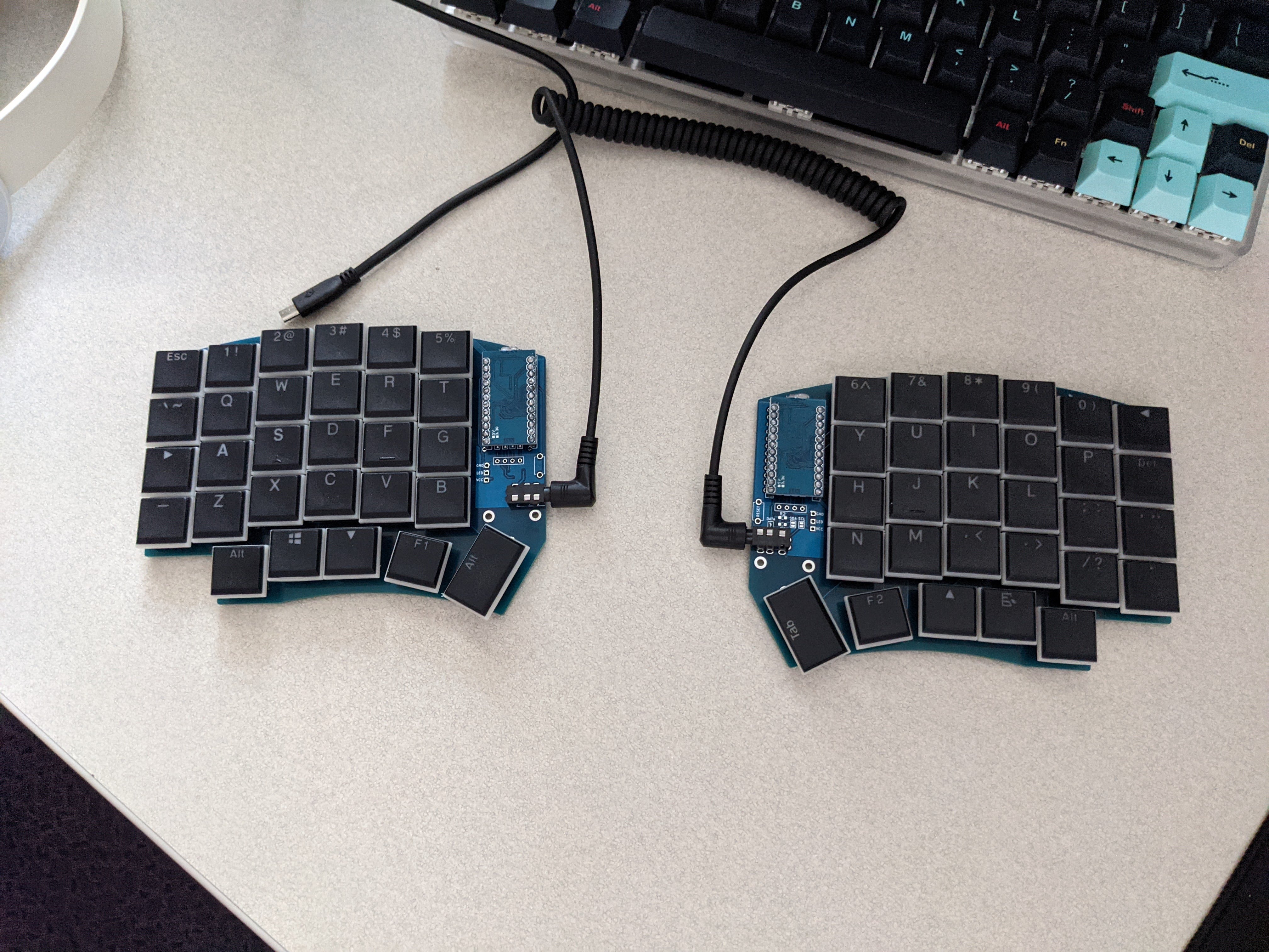
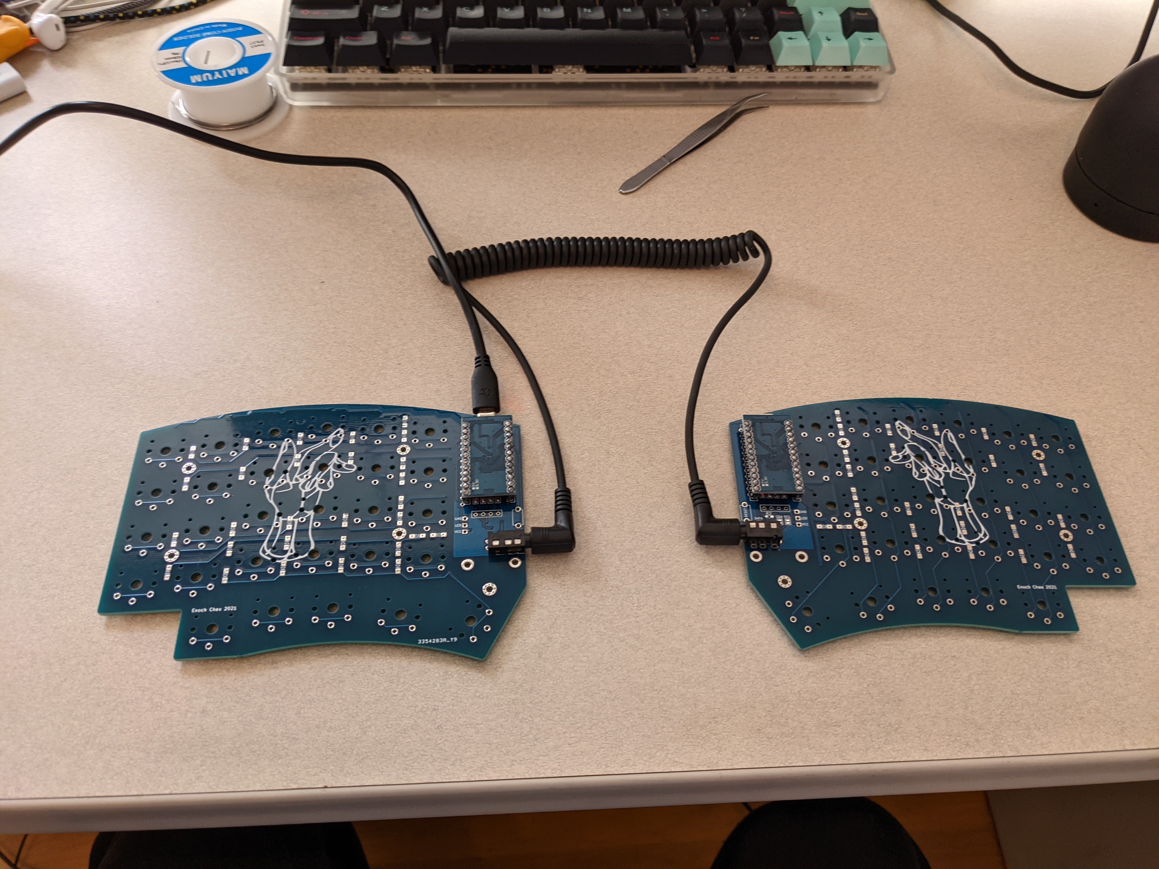
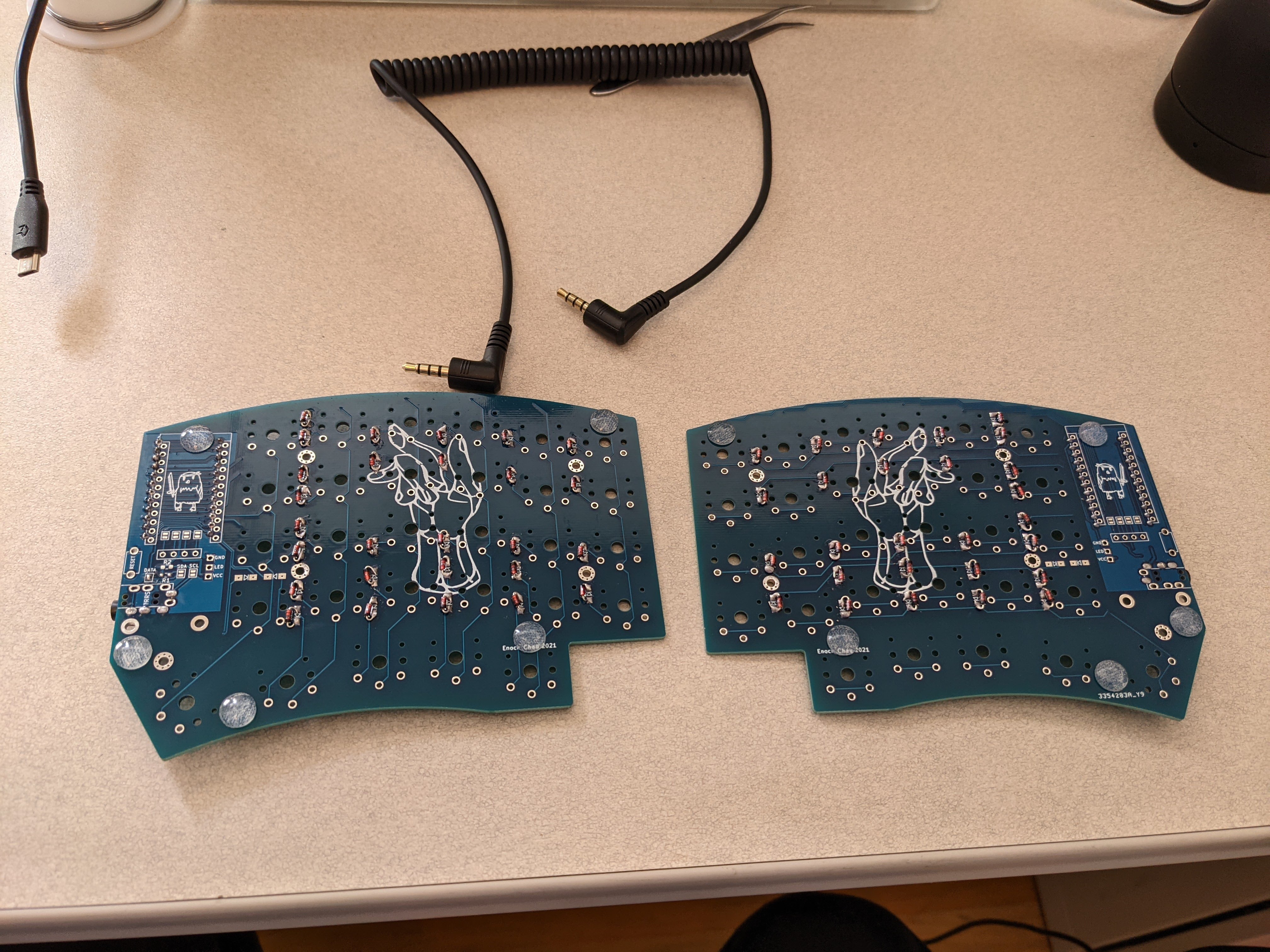
Split lo-profile ergo keyboard
GIS is an open-source printed circuit board by enochchau, from the enochchau/GIS repository on GitHub. It is a 2-layer board of 132.5 × 209.9 mm with 85 parts on 57 nets, routed with 757 tracks and 43 vias.
Its parts include 29 diodes, 29 switches, 3 connectors, 2 resistors and 1 IC. It belongs with the AVR (ATmega, ATtiny) boards of this library.
GIS is a recursive acronym that stands for "GIS is split"
| Qty | Value | Footprint | References |
|---|---|---|---|
| 29 | D | choc:D3_TH_SMD_v2 | D1, D2, D10, D11, D12, D13, D14, D15, D16, D17, D18, D19, D20, D21, D22, D23 +13 |
| 29 | SW_PUSH | choc:Kailh-PG1350-1u-reversible-flip | SW1, SW2, SW10, SW11, SW12, SW13, SW14, SW15, SW16, SW17, SW18, SW19, SW20, SW21, SW22, SW23 +13 |
| 11 | Jumper_NO_Small | SofleKeyboard-footprint:Jumper | JP_DATA1, JP_SCL1, JP_SDA1, JP1, JP2, JP3, JP4, JP5, JP6, JP7, JP8 |
| 5 | HOLE | MountingHole:MountingHole_2.2mm_M2_Pad_Via | TH3, TH4, TH5, TH6, TH7 |
| 2 | 4.7k | Resistor_SMD:R_0603_1608Metric_Pad0.98x0.95mm_HandSolder | R1, R2 |
| 2 | HOLE | SofleKeyboard-footprint:M2_HOLE_PCB | TH1, TH2 |
| 1 | 4PIN | SofleKeyboard-footprint:MJ-4PP-9 | J2 |
| 1 | LED | SofleKeyboard-footprint:LED | J1 |
| 1 | LOGO | art:birb | G*** |
| 1 | LOGO | art:hand_dual | G*** |
| 1 | OLED | SofleKeyboard-footprint:OLED_4Pin | J3 |
| 1 | ProMicro | SofleKeyboard-footprint:ProMicro | U1 |
| 1 | SW_RST | SofleKeyboard-footprint:TACT_SWITCH_TVBP06 | RSW1 |
It measures 132.5 × 209.9 mm and has 2 copper layers, 1.6 mm thick.
85 parts. The full list of its parts is on this page, with links to each part's symbol and footprint where PCBKit's library has them.
From the enochchau/GIS repository on GitHub, at the commit this page was made from: the board is src/PCB/GIS.kicad_pcb. PCBKit opens the board in the browser, with nothing to install.
Its repository states no licence, so its author keeps all rights: ask enochchau before reusing the design.


marksard/Keyboards
This repository is warehouse of my keyboard architecture.
numato/samplecode
This repository contains sample code for different Numato Lab products

BerkeleyHCI/PolymorphicBlocks
A Python-based hardware description language for PCBs for higher-level (block-diagram / system-architecture level) PCB design through libraries of directly reusable subcircuit generators.

jimmerricks/humla
The Humla is a 36-key low profile keyboard based on the Reviung by gtips and the Rev-lp by cyril279. It is for choc switches (with 18x17mm spacing) and has basic support for bluetooth pro micro alternatives such as the…
