Skip to the content
PCBKitNew board
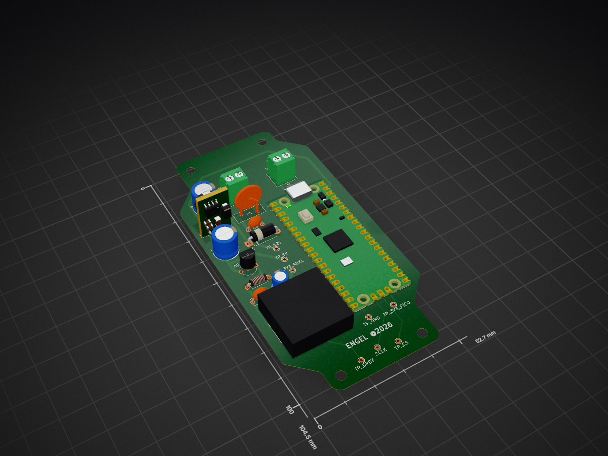
2 layers52.7 × 104.5 mmNode rev.2, the printed circuit board in 3D

Working notes for the first custom RP2350A board with ADXL355, USB-C development power/data, 12 V field input, RS485, and a power architecture biased toward a clean accelerometer supply.
Size
52.7 × 104.5 mm
Copper layers
2
Thickness
0.19 mm
Parts
26
Nets
43
Pads
97
Tracks, vias
82, 0
Pours
1
Routed
Yes
KiCad
KiCad 10.0 (file 20260206)
Created
21 May 2026
Updated
28 Oct 2026

Overview

Node rev.2 is an open-source printed circuit board by engelberd, from the engelberd/sensor-system repository on GitHub. It is a 2-layer board of 52.7 × 104.5 mm with 26 parts on 43 nets, routed with 82 tracks and 0 vias.

It is built around the MF-R050. Its parts include 5 capacitors, 2 ICs, 2 connectors, 1 diode and 1 inductor. It belongs with the RP2040 boards of this library.

Main components

1

README

hardware/Node rev.3.5/README.md

RP2350 ADXL355 node hardware notes

Working notes for the first custom RP2350A board with ADXL355, USB-C development power/data, 12 V field input, RS485, and a power architecture biased toward a clean accelerometer supply.

Design goals

  • Keep firmware changes small by staying close to Raspberry Pi Pico 2/RP2350A.
  • Give ADXL355 the quietest practical supply and layout environment.
  • Allow development from USB-C without a 12 V supply.
  • Allow normal field operation from 12 V.
  • Prevent backfeeding between USB VBUS and the 12 V/buck input.
  • Keep the schematic easy to manufacture externally, even if components are small.

Proposed power tree

text
12V_IN
  -> input fuse/PTC
  -> TVS to GND
  -> reverse polarity protection
  -> TPS62175 buck, 12 V to 5V_BUCK

USB-C VBUS
  -> optional fuse/filter
  -> TPS2121 IN2

5V_BUCK
  -> TPS2121 IN1

TPS2121 OUT = 5V_SYS
  -> TLV75733 -> 3V3_DIG
  -> low-noise LDO -> 3V3_ADXL_PRE
      -> ferrite / 0R option -> 3V3_ADXL

Recommended source priority:

  • IN1: 5V_BUCK from 12 V, main/field source.
  • IN2: USB_5V, fallback/development source.
  • OUT: 5V_SYS.

This means that when both 12 V and USB-C are connected, the board should run from 12 V while USB is used for data/debug. Exact TPS2121 priority and threshold resistors must be set from the datasheet during schematic entry.

Candidate BOM and KiCad mapping

BlockCandidate partKiCad symbolKiCad footprint
MCURP2350AMCU_RaspberryPi:RP2350APackage_DFN_QFN:QFN-60-1EP_7x7mm_P0.4mm_EP3.4x3.4mm_ThermalVias
QSPI flashW25Q128JVS, 16 MiB, SOIC-8Memory_Flash:W25Q128JVS if available, otherwise import/vendor symbolPackage_SO:SOIC-8_3.9x4.9mm_P1.27mm
AccelerometerADXL355BEZ-RL7, LCSC C515892local ADXL355BEZlocal E-14-1_ADI
Input PTCPTS181212V150Device:Fuse / Device:Polyfuselikely Fuse:Fuse_1812_4532Metric or vendor footprint
Input TVSSM6T12ADiode:TVSusually SMB/SMA package; verify exact package before layout
Reverse protectionSS14-E3/61T, LCSC C47460Diode:Schottkyusually Diode_SMD:D_SMA / verify exact package
Buck 12 V to 5 VTPS62175DQCR, LCSC C32097Regulator_Switching:TPS62175DQCuse TI DQC/VSON-10 footprint; verify against datasheet
Power muxTPS2121RUXR, LCSC C485916local TPS2121RUXRlocal RUX0012A
3V3_DIG LDOTLV75733Regulator_Linear:TLV75733PDBV or package-specific variantPackage_TO_SOT_SMD:SOT-23-5 for DBV variant
3V3_DIG alternativeAP2112K-3.3Regulator_Linear:AP2112K-3.3Package_TO_SOT_SMD:SOT-23-5
3V3_ADXL LDOTPS7A2033 or ADP150-3.3Regulator_Linear:TPS7A20xxxDBV or imported ADP150Package_TO_SOT_SMD:SOT-23-5 or exact vendor package
ADXL supply filterMPZ2012S601AT000, 600R @ 100 MHz, 0805Device:Ferrite_BeadInductor_SMD:L_0805_2012Metric
RS485 TVSCDSOT23-SM712Diode:SM712_SOT23Package_TO_SOT_SMD:SOT-23
RS485 transceiverTHVD1450DRInterface_UART:THVD1450DRPackage_SO:SOIC-8_3.9x4.9mm_P1.27mm
USB ESDUSBLC6-2SC6 or TPD2EUSB30Power_Protection:USBLC6-2SC6 / Power_Protection:TPD2EUSB30package-specific SOT-23-6 / X2SON, verify selected part
USB-C connectorselect exact vertical USB-C partConnector:USB_C_Receptacle_USB2.0_16Pselect exact manufacturer footprint

Local downloaded libraries already found:

text
ADXL355 symbol:
/Users/anone/Downloads/ul_ADXL355BEZ/KiCADv6/2026-05-26_12-26-55.kicad_sym

ADXL355 footprints:
/Users/anone/Downloads/ul_ADXL355BEZ/KiCADv6/footprints.pretty/E-14-1_ADI.kicad_mod
/Users/anone/Downloads/ul_ADXL355BEZ/KiCADv6/footprints.pretty/E-14-1_ADI-L.kicad_mod
/Users/anone/Downloads/ul_ADXL355BEZ/KiCADv6/footprints.pretty/E-14-1_ADI-M.kicad_mod

TPS2121 symbol:
/Users/anone/Downloads/ul_TPS2121RUXR/KiCADv6/2026-05-26_13-55-57.kicad_sym

TPS2121 footprint:
/Users/anone/Downloads/ul_TPS2121RUXR/KiCADv6/footprints.pretty/RUX0012A.kicad_mod

Input power schematic notes

Initial 12 V input chain:

text
J_PWR.1 = +12V_IN_RAW
J_PWR.2 = GND

+12V_IN_RAW -> F1 PTC -> +12V_PROT
+12V_PROT -> D_TVS -> GND
+12V_PROT -> D_REV Schottky series -> +12V_SAFE
+12V_SAFE -> TPS62175 VIN

Notes:

  • PTS181212V150 is acceptable for a controlled 12 V lab input, but consider a higher voltage-rated fuse/PTC for field or industrial-style inputs.
  • SM6T12A is aggressive for nominal 12 V. It is fine for a well-controlled 12 V adapter, but for systems that can sit above 12 V, consider a 15 V or 18 V working-voltage TVS while keeping the TPS62175 28 V input limit safe.
  • SS14 as a series reverse-protection diode is simple and acceptable for V1. A P-MOS/ideal-diode style reverse protector would reduce voltage drop and heat.

Buck notes: TPS62175DQCR

Target output: 5V_BUCK.

Required schematic items:

  • VIN input ceramic capacitor close to VIN/GND.
  • Additional optional bulk capacitor footprint near the protected 12 V input.
  • Inductor from SW to 5V_BUCK, selected from TPS62175 datasheet guidance.
  • Output capacitor close to inductor/output return.
  • Feedback divider for 5 V output.
  • EN tied to +12V_SAFE or configured with UVLO if desired.
  • PG routed to a testpoint or left according to datasheet recommendation.
  • Testpoint on 5V_BUCK.

Layout priority:

  • Keep the buck hot loop tiny.
  • Keep SW copper small and away from ADXL355.
  • Place buck, inductor, and high-current input/output caps away from the accelerometer side of the board.

USB-C and power mux notes

USB-C development connector:

text
VBUS -> USB_5V
GND  -> GND
CC1  -> 5.1k -> GND
CC2  -> 5.1k -> GND
D+   -> USB ESD -> RP2350 USB_DP
D-   -> USB ESD -> RP2350 USB_DM

Power mux:

text
TPS2121 IN1 <- 5V_BUCK
TPS2121 IN2 <- USB_5V
TPS2121 OUT -> 5V_SYS
TPS2121 GND -> GND

Do not leave TPS2121 control pins floating. Configure:

  • priority / mode selection,
  • input overvoltage thresholds,
  • current limit,
  • status output if useful.

Exact resistor values should be calculated directly from the TPS2121 datasheet.

3.3 V rails

Digital rail:

text
5V_SYS -> TLV75733 -> 3V3_DIG

3V3_DIG powers:

  • RP2350A I/O and support circuitry,
  • W25Q128JVS flash,
  • RS485 transceiver logic supply,
  • status LED,
  • digital pull-ups and test circuitry.

Analog/accelerometer rail:

text
5V_SYS -> low-noise LDO -> 3V3_ADXL_PRE
3V3_ADXL_PRE -> MPZ2012S601AT000 / 0R option -> 3V3_ADXL
3V3_ADXL -> ADXL355 VDD and VDDIO

Recommendation:

  • Use TLV75733 for 3V3_DIG.
  • Use a low-noise LDO such as TPS7A2033 or ADP150-3.3 for 3V3_ADXL.
  • Keep the ferrite footprint, but make it replaceable by 0R in case the filter resonates with ceramic capacitors or is unnecessary.

Unreleased custom-board pin plan

Despite the historical directory name, this in-progress schematic is not the source of truth for the V2 boards installed in Sanok. The installed V2 pin map is maintained in node/config/board_profile.h.

Keep the first custom board close to the current firmware pinout.

ADXL355 SPI:

text
SCK  -> GPIO10
MOSI -> GPIO11
MISO -> GPIO12
CS   -> GPIO13
DRDY -> GPIO14
INT1 -> GPIO15

RS485:

text
UART TX -> GPIO0
UART RX -> GPIO1
DE      -> GPIO2

This minimizes firmware changes during bring-up.

ADXL355 layout notes

  • Place ADXL355 away from the buck inductor, SW node, USB connector, and RS485 cable connector.
  • Do not route fast digital traces under the sensor.
  • Keep SPI traces short and calm; avoid unnecessarily high drive strength.
  • Put local decoupling very close to ADXL355 supply pins.
  • Keep a continuous ground plane under and around the sensor area.
  • Consider mechanical placement early: the accelerometer measures the board and mounting structure, not just the electrical design.

RS485 notes

Basic RS485 block:

text
3V3_DIG -> THVD1450DR VCC
RP2350 UART_TX -> D
RP2350 UART_RX <- R
RP2350 GPIO_DE -> DE and /RE control as desired
A/B -> connector
A/B -> CDSOT23-SM712 -> GND
Optional 120R termination across A/B via jumper or DNP resistor
Optional failsafe bias resistor footprints if needed

Use 3V3_DIG, not 3V3_ADXL, for RS485.

Items to verify before PCB release

  • RP2350A footprint and exposed pad dimensions against the current Raspberry Pi hardware design files.
  • ADXL355 land pattern against Analog Devices package drawing.
  • Exact USB-C vertical connector part and matching footprint.
  • TPS62175 DQC footprint and feedback/inductor/capacitor values.
  • TPS2121 resistor configuration for priority, input thresholds, and current limit.
  • Flash footprint/package for the selected W25Q128JVS ordering suffix.
  • TVS working voltage against real 12 V input tolerance.
  • Whether the field input should tolerate 24 V mistakes or only regulated 12 V.

Parts

26
QtyValueFootprintReferences
4MountingHoleMountingHole:MountingHole_3.2mm_M3H1, H2, H3, H4
2100nFCapacitor_THT:C_Disc_D5.0mm_W2.5mm_P5.00mmC3, C6
2Screw_Terminal_01x02TerminalBlock_4Ucon:TerminalBlock_4Ucon_1x02_P3.50mm_HorizontalJ1, J2
110uFCapacitor_THT:CP_Radial_D5.0mm_P2.00mmC4
1220uFCapacitor_THT:CP_Radial_D8.0mm_P3.50mmC2
1470uFCapacitor_THT:CP_Radial_D8.0mm_P3.50mmC5
1FRH035080-AInductor_THT:L_Axial_L5.3mm_D2.2mm_P7.62mm_Horizontal_Vishay_IM-1L1
1LP2950CZ-3.3/NOPBPackage_TO_SOT_THT:TO-92_Inline_WideU2
1MF-R050Fuse:Fuse_BelFuse_0ZRE0016FF_L9.9mm_W3.8mmF1
1OKI-78SR-5_1_5-W36-CConverter_DCDC:Converter_DCDC_Murata_OKI-78SR_VerticalU1
1P6KE15A-DIODiode_THT:D_DO-15_P10.16mm_HorizontalD1
1RaspberryPi_PicoModule:RaspberryPi_Pico_Common_UnspecifiedPICO1
1SCLKTestPoint:TestPoint_THTPad_D1.5mm_Drill0.7mmTP8
1TP_12VTestPoint:TestPoint_THTPad_D1.5mm_Drill0.7mmTP3
1TP_3V3_ADXLTestPoint:TestPoint_THTPad_D1.5mm_Drill0.7mmTP6
1TP_3V3_PICOTestPoint:TestPoint_THTPad_D1.5mm_Drill0.7mmTP7
1TP_5VTestPoint:TestPoint_THTPad_D1.5mm_Drill0.7mmTP1
1TP_CSTestPoint:TestPoint_THTPad_D1.5mm_Drill0.7mmTP9
1TP_DRDYTestPoint:TestPoint_THTPad_D1.5mm_Drill0.7mmTP10
1TP_GNDTestPoint:TestPoint_THTPad_D1.5mm_Drill0.7mmTP2
1~Footprints:EVAL-ADXL355ZMOD1

Questions

How big is the Node rev.2 PCB?

It measures 52.7 × 104.5 mm and has 2 copper layers, 0.19 mm thick.

What parts does the Node rev.2 use?

26 parts, built around the MF-R050. The full list of its parts is on this page, with links to each part's symbol and footprint where PCBKit's library has them.

Where can I download the Node rev.2 KiCad files?

From the engelberd/sensor-system repository on GitHub, at the commit this page was made from: the board is hardware/Node rev.2/Node rev.2.kicad_pcb and its schematic hardware/Node rev.2/Node rev.2.kicad_sch. PCBKit opens the board in the browser, with nothing to install.

Can I use the Node rev.2 design in my own project?

Its repository states no licence, so its author keeps all rights: ask engelberd before reusing the design.

More from engelberd/sensor-system

1
  • 4 layers51.4 × 31.4 mmRP2350, the printed circuit board in 3D

    RP2350

    engelberd/sensor-system

    Working notes for the first custom RP2350A board with ADXL355, USB-C development power/data, 12 V field input, RS485, and a power architecture biased toward a clean accelerometer supply.

    87 parts2

Similar boards

  • 2 layers85 × 155 mmEsp32-fan controller, the printed circuit board in 3D

    Esp32-fan controller

    merlindorin/esp32-fan-controller

    A small KiCad board to keep my home server cabinet cool. 4 PWM fans, 4 temperature probes, one ESP32.

    38 parts8MIT
  • 2 layers68.6 × 88.4 mmShield coil winder, the printed circuit board in 3D

    Shield coil winder

    jonathan-iap/CoilWinder

    A reprap coil winder machine based on arduino language

    34 parts4GPL-3.0
  • 2 layers72.1 × 41.8 mmPower injector rev c, the printed circuit board in 3D

    Power injector rev c

    grodansparadis/can4vscp-power-injector

    Power injector module for CAN4VSCP

    28 parts2
  • 2 layers100 × 100 mmTesseract, the printed circuit board in 3D

    Tesseract

    IoTCloudStudio/HW_Develop

    89 parts2
  • 2 layers120.4 × 100.1 mmDP1600i, the printed circuit board in 3D

    DP1600i

    Hocus-Pocus/Speeduino-DP1600i-

    126 parts1
  • 2 layers30 × 58.5 mmLoragate tht, the printed circuit board in 3D

    Loragate tht

    andrewgho/loragate

    ESP32 + LoRa radio powered reed switch door sensor

    10 parts
  • 2 layers100 × 100 mmFishy8, the printed circuit board in 3D

    Fishy8

    EmanuelKrabNL/Fishy8

    PCB with vintage camera looking footage. A microphone and a fisheye lens.

    15 partsMIT