
2 layers22.5 × 110.8 mm

My version of an LCD Backpack with some unique features
E1201 is an open-source printed circuit board by Electro707, from the Electro707/p1200_lcd_backpack repository on GitHub, published under the GPL-3.0 licence. It is a 2-layer board of 63 × 34.5 mm with 54 parts on 57 nets, routed with 537 tracks and 194 vias.
It is built around the TPS61222DCK, LM2776DBV and TCA9517ADGK, with the TXU0202DCU, TXU0304PW and MMBF170 among its other parts. Its parts include 14 resistors, 10 capacitors, 8 connectors, 6 ICs and 3 diodes. It belongs with the lEDs and displays boards and the PIC boards of this library.


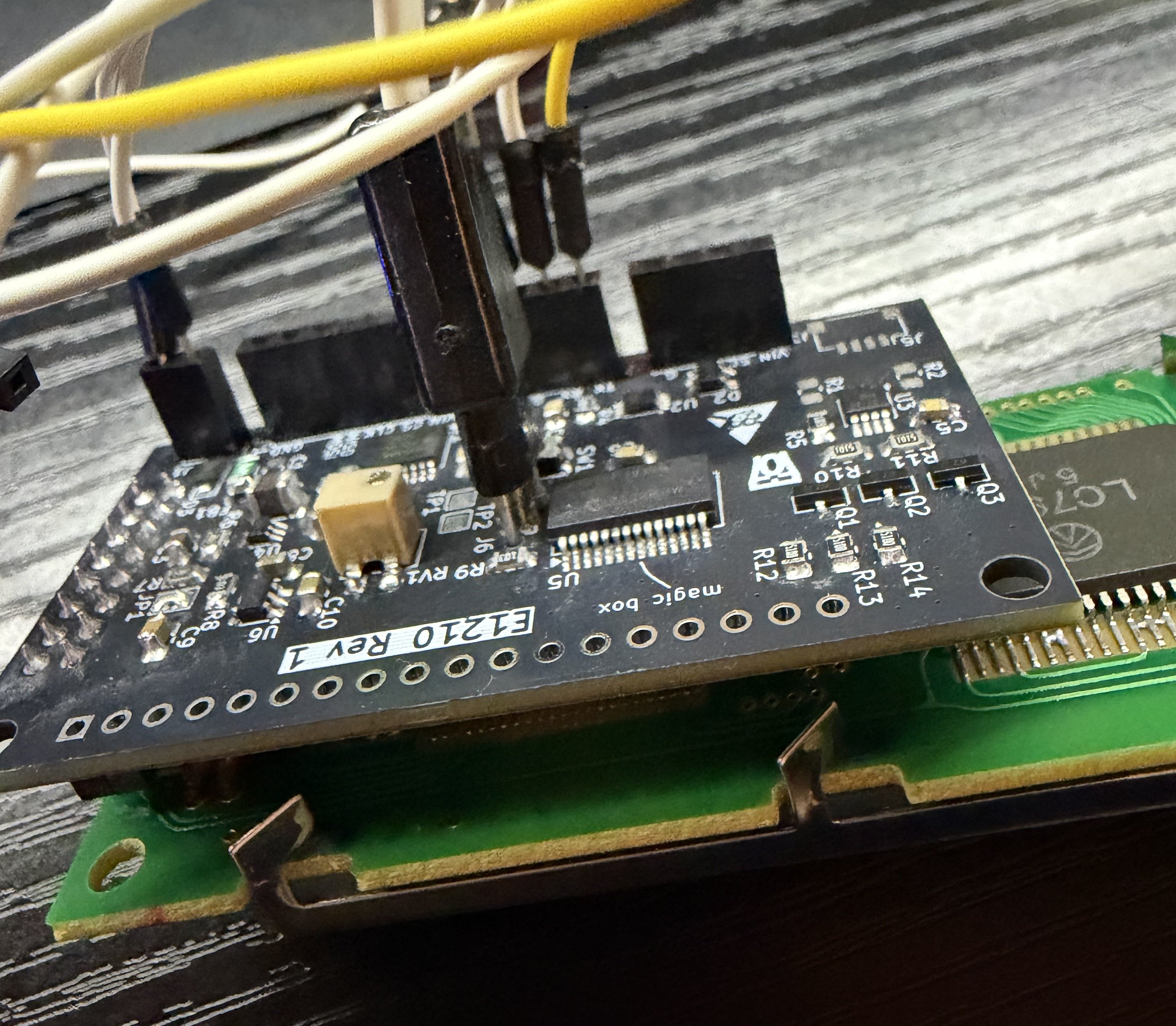 Image of board on an LCD during development
This project is for a generic LCD backpack, similar to the many ones out there, with some distinct features that lead me to build my own:
TODO: this section
The ERRATA's for the latest revision PCB can be found in ERRATA.md
The firmware for this project is targeted towards the MCU on board (PIC16F18155).
To use the project, open it up in MPLAB IDE (v6.35 used), with PIC-AS 4.00 (comes with XC8) and device pack PIC16F1xxxx_DFP==1.31.465 (other version should be OK, noted for repeatability).
The project is written in assembly. Why? Why not? This was mostly for my learning of writing an entire firmware in bare assembly and getting familiar with the PIC architecture. I found it fun.
More info on the firmware, including the communication protocol, can be found in F1202/README.md
This project is licensed under GPLv3**
** This excludes the files in E1201/SparkFun-Qwiic.pretty, as they came from the Sparkfun
| Qty | Value | Footprint | References |
|---|---|---|---|
| 5 | 10k | Resistor_SMD:R_0805_2012Metric_Pad1.20x1.40mm_HandSolder | R3, R4, R5, R8, R9 |
| 4 | 100nF | Capacitor_SMD:C_0805_2012Metric_Pad1.18x1.45mm_HandSolder | C2, C4, C5, C6 |
| 4 | 5.1k | Resistor_SMD:R_0805_2012Metric_Pad1.20x1.40mm_HandSolder | R1, R2, R10, R11 |
| 3 | 510 | Resistor_SMD:R_0805_2012Metric_Pad1.20x1.40mm_HandSolder | R12, R13, R14 |
| 3 | MMBF170 | Package_TO_SOT_SMD:SOT-23 | Q1, Q2, Q3 |
| 2 | 10uF | Capacitor_SMD:C_0805_2012Metric_Pad1.18x1.45mm_HandSolder | C3, C7 |
| 2 | 2.2uF | Capacitor_SMD:C_0805_2012Metric_Pad1.18x1.45mm_HandSolder | C8, C10 |
| 2 | Conn_01x04_Socket | Connector_PinSocket_2.54mm:PinSocket_1x04_P2.54mm_Vertical | J2, J3 |
| 2 | ESDA14V2SC5 | Package_TO_SOT_SMD:SOT-23-5 | D1, D2 |
| 2 | MountingHole | MountingHole:MountingHole_3.2mm_M3 | H1, H2 |
| 2 | TestPoint | TestPoint:TestPoint_Pad_1.5x1.5mm | TP1, TP2 |
| 1 | 100pF | Capacitor_SMD:C_0805_2012Metric_Pad1.18x1.45mm_HandSolder | C1 |
| 1 | 10k | Potentiometer_SMD:Potentiometer_Bourns_3214X_Vertical | RV1 |
| 1 | 180k | Resistor_SMD:R_0805_2012Metric_Pad1.20x1.40mm_HandSolder | R7 |
| 1 | 1uF | Capacitor_SMD:C_0805_2012Metric_Pad1.18x1.45mm_HandSolder | C9 |
| 1 | 20k | Resistor_SMD:R_0805_2012Metric_Pad1.20x1.40mm_HandSolder | R6 |
| 1 | 4.7uH | Inductor_SMD:L_1210_3225Metric | L1 |
| 1 | 500mA | Fuse:Fuse_1206_3216Metric_Pad1.42x1.75mm_HandSolder | F1 |
| 1 | Conn_01x06_Socket | Connector_PinSocket_2.54mm:PinSocket_1x06_P2.54mm_Vertical | J4 |
| 1 | Conn_01x18 | Connector_PinSocket_2.54mm:PinSocket_1x18_P2.54mm_Vertical | J8 |
| 1 | Conn_02x08_Odd_Even | Connector_PinHeader_2.54mm:PinHeader_2x08_P2.54mm_Vertical | J7 |
| 1 | FerriteBead | Inductor_SMD:L_0805_2012Metric_Pad1.05x1.20mm_HandSolder | FB1 |
| 1 | ICSP | Connector:Tag-Connect_TC2030-IDC-NL_2x03_P1.27mm_Vertical | J6 |
| 1 | Jumper_2_Open | Jumper:SolderJumper-2_P1.3mm_Open_TrianglePad1.0x1.5mm | JP1 |
| 1 | LM2776 | Package_TO_SOT_SMD:SOT-23-6 | U6 |
| 1 | PIC16F18154-xSP | Package_SO:SSOP-28_5.3x10.2mm_P0.65mm | U5 |
| 1 | QWIIC | Connector_JST:JST_SH_SM04B-SRSS-TB_1x04-1MP_P1.00mm_Horizontal | J5 |
| 1 | SMF5V0A | Diode_SMD:D_SMF | D3 |
| 1 | SW_Push | Button_Switch_SMD:SW_Push_1P1T_NO_CK_KMR2 | SW1 |
| 1 | Screw_Terminal_01x02 | Connector_PinSocket_2.54mm:PinSocket_1x02_P2.54mm_Vertical | J1 |
| 1 | TCA9517ADGK | Package_SO:VSSOP-8_3x3mm_P0.65mm | U3 |
| 1 | TPS61222DCK | Package_TO_SOT_SMD:Texas_R-PDSO-G6 | U4 |
| 1 | TXU0202DCU | Package_SO:VSSOP-8_2.3x2mm_P0.5mm | U2 |
| 1 | TXU0304PW | Package_SO:TSSOP-14_4.4x5mm_P0.65mm | U1 |
It measures 63 × 34.5 mm and has 2 copper layers, 1.6 mm thick.
54 parts, built around the TPS61222DCK, LM2776DBV, TCA9517ADGK and TXU0202DCU. The full list of its parts is on this page, with links to each part's symbol and footprint where PCBKit's library has them.
From the Electro707/p1200_lcd_backpack repository on GitHub, at the commit this page was made from: the board is E1201/E1201.kicad_pcb and its schematic E1201/E1201.kicad_sch. PCBKit opens the board in the browser, with nothing to install.
Its repository publishes it under the GPL-3.0 licence: you may reuse it on that licence's terms (keep the author's notice, and for a copyleft licence share your changes alike).

dg1vs/Transputer-TRAM-TangNano
A TRAM-size FPGA Transputer module based on the Sipeed Tang Nano 20K.

dg1vs/Transputer-Teensy-Link
A family of practical, Ethernet-connected link interfaces for classic INMOS transputer systems, based on the Teensy 4.1.


About-Time-Technologies/MHCI
Modular Hardware Control Interface - Components for the Events Industry

bot-hoven/bot-hoven-electrical
Electrical substem for Bot-Hoven. Includes KiCad files containing schematics and PCB designs for components in Bot-Hoven.

Dhruv2212-star/9-axis-IMU-barometer-Data-logger-
This project is a compact, battery-powered data logger designed to record motion and environmental data in a single device.
