


2 layers50 × 65 mm
RB Pirate
reza-bakhshi/RB-Pirate
RB-Pirate helps developers, makers, and hardware enthusiasts communicate with, analyze, and debug electronic devices directly from a terminal.
247 partsMIT

Physical buttons for media control on the Sony WH-1000XM2, WH-1000XM3, WH-1000XM4 and possibly WH-1000XM5 wireless headphones
Tobo is an open-source printed circuit board by eldstal, from the eldstal/touchless-xm repository on GitHub. It is a 2-layer board of 57.3 × 61 mm with 91 parts on 105 nets, routed with 921 tracks and 113 vias.
It is built around the ATMEGA328P-AN, CH340E and MAXM20343AMP+, with the SKRTLBE010 among its other parts. Its parts include 25 capacitors, 19 resistors, 15 ICs, 7 diodes and 6 connectors. It belongs with the audio and music and interfaces and adapters boards and the AVR (ATmega, ATtiny) boards of this library.


A mod for Sony WH-1000XM2 (experimental), WH-1000XM3, WH-1000XM4 and WH-1000XM5 (experimental) headphones to remove the gesture-based touch controls and add physical buttons.
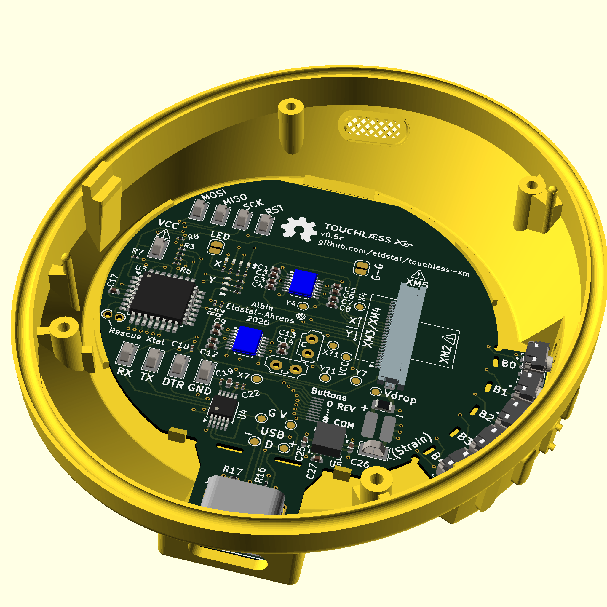
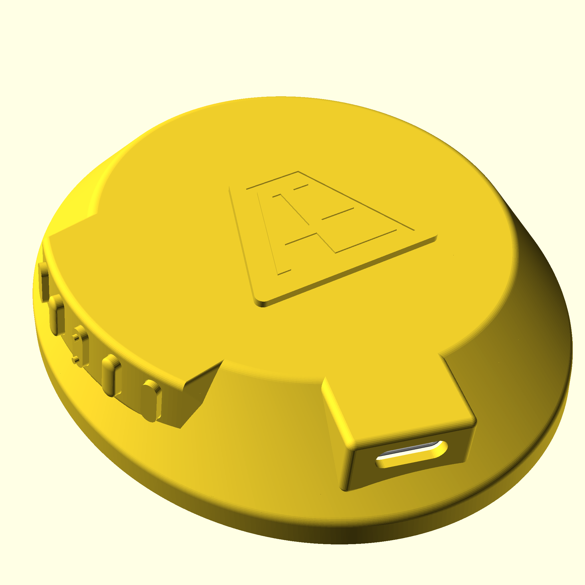
The project is feature-complete and the electronics are functional. I'd call it a Beta product, since I'm the only user and still tweaking the design details.
The design has been 3D-printed and test fit against an XM4 headset. The mic grill looks good but prints awful. Could be that we need to use a metal mesh inserted during the print.
The buttons have different top surfaces, so you can feel which is which. They've also been relocated to be less likely to be accidentally actuated.
STLs will be available both with and without USB ports, with and without the Æ logo.
v0.5c of the board has been manufactured and works great!
I've installed it in my own headset for some day-to-day testing.
Ready to go. USB support (only for programming) is already included in the main board. The project uses platform.io and OptiBoot to run an Arduino-based firmware.
I only have a pair of XM4 to test with, so the design is made to fit them. The connector is a 24-pin, but only XM5 has a cable that wide. For other models, insert your narrower cable carefully to match the lines on the PCB.
I've laid out the board for experimental support for the XM2. These are the most different out of the bunch, so there are caveats.
⚠️WARNING⚠️ The OEM cable will not work, because the XM2 has the touch board's connector at the front. You will need a slightly longer cable with opposite side contacts. Possibly This Würth 687712100002 is suitable, but too long of a cable will cause interference. If you can trim it to length, that will improve the chances of success.
There is no bespoke connector for the XM2, you need to very carefully position it in the larger connector using the lines on the PCB.
It's also necessary to modify the firmware pin map slightly, since the Y pins are in the opposite order. Use --environment xm2 when you compile the firmware.
If you've got a pair of XM2s and want to help me tune the compatibility, let me know!
The XM3 touch board and battery connector appear to be electrically identical to XM4, so the PCB should be compatible. A different case design may be needed.
Insert your cable all the way at the top of the connector (there will be two unused pins at the bottom). Follow the lines in the silkscreen for guidance.
The project is designed for these, so these will be the ones primarily tested. The OEM touch board has a flat cable which Touchlæss is designed to reuse.
Insert your cable all the way at the top of the connector (there will be two unused pins at the bottom). Follow the lines in the silkscreen for guidance.
The battery uses a 2-pin JST ZH series connector. There is no vertical space inside the case for a matching connector on the board, so I've resorted to soldering a Y-connector onto the Touchlæss pcb. Separate from the PCB BOM, you'll need one male and one female JST ZH-2 connector and some red/black cables.
Experimental support is included in the initial board design, but I do not own a pair of XM5 and cannot test them. The XM5 pinout is entirely based on reverse-engineering of photos, so I may have made a mistake! The Touchless board shouldn't be able to do any damage to the headphones. If you have a pair of XM5s and would like to help me test the compatibility, feel free to reach out!
At a minimum, the XM5 OEM design doesn't include a loose cable for us to reuse. You will need a suitable flat cable, which is 24-pin FFC with 0.5mm pitch and same-side connectors. This Würth 687624050002 should work, but may not be the proper length.
The battery connector for XM5 is also different, a 3-pin of unknown design. If you have more information about this, let me know!
With any luck, the XM6 touch board will be similar to the XM5. It will be a while before I get my hands on a new high-end headset to test it, though.
If you're getting a pair of XM6 and would like to send me some nice photos of the internals, I'll be very grateful!
Highly unlikely. At the very least, you'll need to figure out the pinout for the touch sensor board. Most likely there will be other things that need tuning as well. If you want to make something like touchless for a different headset, take a look at the technical documentation for some pointers on how Touchless works.
Not really. When idle, the board draws about 0.02 mA. When you're actively pressing/holding buttons it peaks at just under 13mA. This is on the order of one LED, and only when you're actively pushing buttons.
The DC converter on the board will stop working once the battery drops below about 0.7V, which is quite a bit before the headphones actually stop working. That means the buttons won't work when your battery is very low.
That's OK, it's only needed for development (reprogramming the Touchless board without disassembling the headphones). Simply snap the USB connector off from the main board (see perforations) and print yourself a case without a USB block. Set cap_type=nousb in xm4-cap.scad to get a case that's closed at the bottom.
That's no problem! Snap the button portion off of the main board (see perforations) and use the solder points on the front or back to connect your own buttons placed wherever you want them. If you're keen on PCB design, it's not that hard to redesign the PCB for button placement (or add/remove buttons as needed).
There is no need for external resistors etc, just connect a switch between one button contact and the COM and you're good to go.
No problem! If you remove the buttons and the USB addition (see above), the touchless board should fit inside the OEM ear cup (you have to remove the original touch board first, which may be destructive). Make cuts in the case as needed to mount buttons where you want them, and wire them up to the exposed button solder points on the front or back of the PCB.
Easiest way to do this is in the firmware. Take a look at buttonmap.cpp to switch and swap however you like. You'll need the included USB port or a serial cable to program the board after you've made your modifications. Instructions are down below.
The board itself works as its own development board, of sorts. If you're going to be flashing new software via USB while testing, I recommend connecting the USB V (+5v) pad to the VCC test point as shown in this photo. If you also short out the "LED" solder bridge you get LED indications of which touch points are currently being "touched".
Please disconnect the USB power jumper before installing in the headset and connecting a battery
Great! You can find the dimensions of the PCB here. It's all relative to the center of the circular area, so if your CAD program supports polar coordinates you'll have an easier time of it. You may also have use for make vrml in the pcb directory, which creates a VRML 3D export of the PCB to use as a reference in your model.
That won't be possible, sorry. Touchlæss only works by simulating touches and swipes, so it can only do what the headphones allow you to do with the touch panel.
Yes. There is a significant delay between pushing a button and the headset responding. This isn't something we can control, since Touchlæss simulates touch gestures. If a swipe takes 120ms to perform, the headset can't react sooner than that.
That will be an adventure. Touchlæss interfaces with the board in the right cup, so you'll need to run wires across the headband to get to the other side. Not impossible, but certainly a lot of work.
That's great! I won't ask for any royalties or whatever. If you do set something up, I'm happy to include a link here so people can buy from you.
Note: The VCC loop on the PCB is powered by the headset battery via a step up/step down converter configured for 3.3V. Do not connect an external supply to this hook while the battery is connected. The loop is only needed in order to program and test the board without a headset connected.
The board will not take power from the USB connector by default. If you want to power it via USB while programming, connect a jumper between the USB V test point and the VCC test point as illustrated here. Disconnect that jumper again before connecting a battery, please.
This only needs to be done once per board
When you have a fresh board with a factory-stock microcontroller, you'll have to start with the bootloader. For this step you need a hardware AVR programmer, for example:
...or anything else supported by avrdude or platform.io. Install the platform.io tools and let's go!
| tobo | AVRISP 10-pin | Glasgow | BP harness |
|---|---|---|---|
| MOSI | 1 | PURP | 8 Pink |
| VCC | 2 | ORG | 2 White |
| RST | 5 | YEL | 6 Green |
| SCK | 7 | PINK | 7 Yellow |
| MISO | 9 | BRN | 10 Brown |
| GND | 10 | B/W | 1 Black |
If you're using a new kind of programmer, add the needed environment to firmware/tobo/platformio.ini to use your programmer.
Warning Ensure that your new environment extends env:tobo, so that the frequency and fuses are programmed properly. If you do not, you may need to temporarily connect an external crystal (see PCB markings) in order to recover the board.
cd firmware/tobo
pio run --environment avrispv2 --target bootloader
If there are no errors, congratulations! Your tobo board is an Arduino! You're ready for the next step.
If you've made changes to the code and want to update your board, this step is the only one you need to repeat
If your board has the bootloader installed, you can put your ISP programmer away and use either the on-board USB port or your own serial adapter. This can be an FTDI cable, a different USB-to-serial adapter, or an arduino board with no microcontroller.
Hook up your serial cable to the tobo:
| tobo | serial adapter |
|---|---|
| RX | TX |
| TX | RX |
| GND | GND |
| DTR | DTR (if your cable has it) |
| RST | RST (if using an arduino) |
| VCC | VCC Only if you don't have the battery plugged in |
cd firmware/tobo
pio run --target upload
If all went well, you're ready to go!
I've had the board produced by PCBWay with no issues. The following facts are useful while setting up an order:
The total cost for production, components and assembly of 5 boards was about $280 including shipping to Europe and VAT. That works out to about $56 per board. You can reduce the BOM cost some by removing the USB port, USB-Serial circuitry and the LEDs. You could also save a bit by not populating the test loops, but it will make it more difficult to program the board.
Touchlæss XM © 2026 by Albin Eldstål-Ahrens is licensed under Creative Commons BY-SA 4.0
This means you are free to use, modify, distribute, remix, redesign the project however you wish as long as you
If you want to make and sell kits of this, feel free! If you make money from my work, please consider making a donation to a charitable organization as a thank you!
| Qty | Value | Footprint | References |
|---|---|---|---|
| 14 | 1.5pF | Capacitor_SMD:C_0402_1005Metric | C1, C2, C3, C4, C5, C6, C7, C8, C9, C10, C11, C12, C13, C14 |
| 12 | TestPoint | TestPoint:TestPoint_Pad_D1.0mm | D-1, D+1, USB5, USBG1, V1, V2, X?1, X1, X2, X7, Y?1, Y4 |
| 10 | 5015 | tobo-footprints:5015 | U6, U7, U8, U9, U10, U11, U12, U13, U15, U16 |
| 9 | 1K | Resistor_SMD:R_0201_0603Metric | R1, R2, R3, R4, R5, R6, R7, R8, R20 |
| 7 | 270 | Resistor_SMD:R_0201_0603Metric | R9, R10, R11, R12, R13, R14, R15 |
| 7 | LED | LED_SMD:LED_0201_0603Metric | D1, D2, D3, D4, D5, D6, D7 |
| 5 | SKRTLBE010 | tobo-footprints:SKRTLBE010 | S1, S2, S3, S4, S5 |
| 4 | 0.1uF | Capacitor_SMD:C_0201_0603Metric | C18, C19, C21, C22 |
| 3 | 10uF | Capacitor_SMD:C_0402_1005Metric | C17, C20, C25 |
| 2 | 1.5pF | tobo-footprints:C_Disc_D5.0mm_W2.5mm_P2.50mm | C15, C16 |
| 2 | 5.1K | Resistor_SMD:R_0201_0603Metric | R16, R17 |
| 2 | Conn_01x09_Pin | tobo-footprints:button_breakout_0.5mm | J6, J7 |
| 2 | SolderJumper_2_Open | Jumper:SolderJumper-2_P1.3mm_Open_RoundedPad1.0x1.5mm | JP1, JP2 |
| 2 | ~ | tobo-footprints:VSSOP50P400X100-14N | U1, U2 |
| 1 | 1 | Resistor_SMD:R_0805_2012Metric | R27 |
| 1 | 2.2uF | Capacitor_SMD:C_0402_1005Metric | C27 |
| 1 | 22uF | Capacitor_SMD:C_0402_1005Metric | C26 |
| 1 | 54548-2472 | tobo-footprints:molex-545482472 | J4 |
| 1 | ATmega328P-AN | Package_QFP:TQFP-32_7x7mm_P0.8mm | U3 |
| 1 | CH340E | tobo-footprints:MSOP-10_3x3mm_P0.5mm_narrowpads | U4 |
| 1 | Conn_01x02_Pin | tobo-footprints:power-cable | J2 |
| 1 | Conn_01x09_Pin | tobo-footprints:button_breakout_2.54mm | J5 |
| 1 | Hroparts Elec TYPE-C-31-M-12 | Connector_USB:USB_C_Receptacle_HRO_TYPE-C-31-M-12 | J8 |
| 1 | MAXM20343AMP+ | tobo-footprints:21-100447_ADI | U5 |
It measures 57.3 × 61 mm and has 2 copper layers, 0.6 mm thick.
91 parts, built around the ATMEGA328P-AN, CH340E, MAXM20343AMP+ and SKRTLBE010. The full list of its parts is on this page, with links to each part's symbol and footprint where PCBKit's library has them.
From the eldstal/touchless-xm repository on GitHub, at the commit this page was made from: the board is pcb/tobo/tobo.kicad_pcb and its schematic pcb/tobo/tobo.kicad_sch. PCBKit opens the board in the browser, with nothing to install.
Its repository states no licence, so its author keeps all rights: ask eldstal before reusing the design.
reza-bakhshi/RB-Pirate
RB-Pirate helps developers, makers, and hardware enthusiasts communicate with, analyze, and debug electronic devices directly from a terminal.


wazzeemsha/ATMEGA328P-DataLogger-PCB
4-layer KiCad PCB design of an ATmega328P-AU based microcontroller data logger with dual EEPROMs, RTC, and complete manufacturing-ready Gerber files.

Open-Smartwatch/open-smartwatch-gps
Hardware design files for the GPS version of the open-smartwatch
