2 layers100 × 89.5 mm
Led processor board
eelstretching/led-processor-board
A board with a processor and a couple of other things that can talk to an LED output board.
128 parts

 eelstretching/rp2350b-rm2-reference
Raspberry Pi's RP2350B minimal design (RPI-RP2350B-MINIMAL R4-S1, KiCad 10) with these additions:
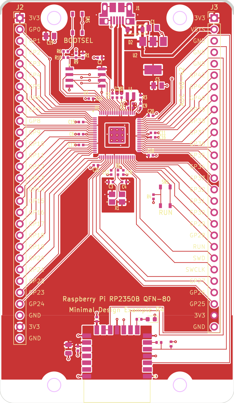
RP2350B RM2 is an open-source printed circuit board by eelstretching, from the eelstretching/rp2350b-rm2-reference repository on GitHub. It is a 2-layer board of 52 × 89.5 mm with 57 parts on 85 nets, routed with 541 tracks and 59 vias.
It is built around the RP2350B, W25Q128JVSIQ and APS6404L-3SQR-SN, with the 10103594-0001LF and B5819W among its other parts. Its parts include 25 capacitors, 14 resistors, 5 ICs, 3 connectors and 2 diodes. It belongs with the RP2350 boards of this library.


Raspberry Pi's RP2350B minimal design (RPI-RP2350B-MINIMAL R4-S1, KiCad 10) with these additions:
That leaves GPIO 0-42 free and in order on the J2/J3 headers, instead of the Pico 2 W's gap at 23/24/25/29.
Status: schematic and layout done, DRC clean, not yet fabricated. See "Layout" for what changed on Pi's board.
| GPIO | Use |
|---|---|
| 0-42 | free, on J2/J3 (0/1 = default UART0) |
| 43 | RM2 WL_ON + BT_ON |
| 44 | RM2 gSPI CS |
| 45 | RM2 gSPI DATA: DI direct, DO through 470R (R14), IRQ through 10k (R15) |
| 46 | RM2 gSPI CLK |
| 47 | PSRAM chip select (XIP_SS_N[1]), 10k pull-up R13, 0R link R11 |
GPIO 43-47 aren't on the headers: they belong to the radio and the PSRAM.
The headers, from the USB end down:
| Header | Top | Middle | Bottom |
|---|---|---|---|
| J2 (left, 29 pins) | 3V3 | GP0-GP24 | GND, 3V3, GND |
| J3 (right, 28 pins) | 3V3, VSYS, GND, GND, GND | GP42-GP28, RUN, SWD, SWCLK, GP27-GP25 | 3V3, GND |
The radio circuit is the Pico 2 W's (and the RM2 datasheet's) on different pins:
CYW43_WL_GPIO_LED_PIN.The cyw43 driver takes any pins from the board header, so nothing else changes in firmware. On the RP2350B a PIO block reaches either GPIO 0-31 or 16-47. The radio's PIO therefore sits in the 16-47 window, which means LED output PIOs for GPIO 0-15 must use a different PIO block.
The board runs from USB, or from 5 V on J3 pin 2 (VSYS), which works like a Pico's VSYS pin.
J2 and J3 are single rows on the 0.1" grid, 1.7" (17 holes) apart, so the module drops straight into perfboard, and every pin has free holes beside it.
Two traps:
With pico-sdk 2.3.0 or later, linking hardware_psram brings the PSRAM up at boot. It reads
PICO_PSRAM_CS_PIN and PICO_PSRAM_SIZE_BYTES, which the board header already sets. The PSRAM then
appears as ordinary memory at 0x11000000.
Static data: __uninitialized_psram("name") (or __in_psram("name") for initialised data)
places a variable or array in PSRAM.
Dynamic allocation: firmware/psram_alloc adds psram_malloc, psram_calloc,
psram_realloc, psram_memalign and psram_free, plus psram_heap_stats(). These work like
malloc (8-byte aligned, safe from both cores, not from interrupt handlers) but allocate from the
PSRAM left after any PSRAM variables. The SDK's own malloc stays in the faster on-chip SRAM.
It's a TLSF allocator with its control block in SRAM. To use it:
add_subdirectory(path/to/firmware/psram_alloc psram_alloc)
target_link_libraries(my_app psram_alloc)
PSRAM is slower than SRAM, so use it for big, mostly-streamed data (frame and pixel buffers, audio,
network buffers). Keep stacks and hot data in SRAM. firmware/psram_test prints the throughput, and
is the first thing to run on a new board to check U4.
| Path | What |
|---|---|
RP2350B-RM2.kicad_sch | schematic (single sheet, A3) |
RP2350B-RM2.kicad_pcb | Pi's R4 layout, 18 mm longer, plus the RM2 and the PSRAM (see "Layout") |
rp2350b_rm2.kicad_sym, rp2350b_rm2.pretty/RPi_RM2.kicad_mod | RM2 symbol and footprint (project libraries, already in sym-lib-table / fp-lib-table) |
bom-jlcpcb.csv | BOM with LCSC numbers |
firmware/boards/rp2350b_rm2.h | pico-sdk board header (CYW43 pins, 16 MB flash, 8 MB PSRAM on GPIO47) |
firmware/blink/ | bring-up test: blinks D1 through the radio, so it proves the RM2 is alive |
firmware/psram_test/ | bring-up test for the PSRAM: tests all 8 MB, measures throughput, exercises the heap |
firmware/psram_alloc/ | psram_malloc() / psram_free(): a heap in PSRAM for your own projects (TLSF, vendored) |
tools/kisch.py, tools/kirender.py | netlist dump/check and rough PNG preview of a schematic, no KiCad needed |
tools/rm2_footprint.py | generator for the RM2 footprint |
tools/update_pcb_from_sch.py, tools/layout_rm2.py | the scripted Update PCB from Schematic and RM2/PSRAM layout pass that produced the board (run once, in KiCad's Python; kept for reference) |
docs/schematic-*.png | rough schematic previews (full sheet, radio, PSRAM) |
docs/pcb-front.png, docs/pcb-back.png | board renders (front copper and silk; back copper, mirrored) |
Every part has an LCSC number except these three:
Passives were swapped from Pi's Murata/Yageo parts to JLC basic equivalents with the same value, size and dielectric. The 100n parts are 16 V instead of 25 V, which is fine on 3.3 V.
The board is Pi's R4 layout with Update PCB from Schematic applied, and the areas below added or changed. Every Pi footprint stays where it was apart from the bottom mounting holes (MH3, MH4) and the headers (J2, J3), which are now single rows on Pi's signal columns. Pi's JST debug connector (J4) is gone, since SWD and SWCLK are on J3. D2 is new, next to the USB connector. Pi's tracks are untouched apart from the U4 fan-out, the R11 stub, the last stretch of GPIO43-47's runs to J3, and SWD/SWCLK where they used to pass through J4. Pi's VBUS pour is split in two around D2.
RM2 end. The board is 18 mm longer (89.5 x 52 mm), and the extra length is at the end away from USB, as on the Pico 2 W. The headers stay on both long edges. The RM2 (U5) sits between them, centred, with its antenna end (pins 1 and 21) at the new bottom edge. The module's top edge clears Pi's "Minimal Design Example R4" silkscreen line.
CYW43_PIO_CLOCK_DIV_INT before suspecting anything else.The gSPI lanes run alongside J3's pins, so expect a little crosstalk from SCLK onto anything wired to J3.
Mounting holes. MH3 and MH4 move from Pi's old bottom edge to the new end of the board, at the same x as the top pair (86.03 and 113.97 mm) and 4 mm from the edge, again like the top pair. The four holes keep Pi's rectangular pattern, now 27.94 x 81.5 mm. The top pair can't move into the true corners because J2/J3 pin 1 is there. At the bottom, the holes flank the RM2's antenna about 5 mm from its ends, as on the Pico 2 W. The antenna rule area allows them because they're NPTH holes with no copper.
Headers. J2/J3 swap Pi's 2x26 Samtec headers for stock 1x29 / 1x28 2.54 mm headers on Pi's inner (signal) columns, so every GPIO keeps its pad and Pi's routing to it. The outer GND column is gone, and the top-layer +3V3 pour and the back GND plane fill its place.
Pi's silkscreen labels for J3's top five pins now read 3V3, VSYS and GND, "ADC 40-47" reads "ADC 40-42", and the "Outer Row GND" notes are gone. The new bottom pins get labels in the same style.
VSYS on J3. D2 (SOD-123) sits between the USB connector, C1 and U2, in what was Pi's VBUS pour. That pour is split in two. A small USB-side piece runs from J1's VBUS pin to D2's anode, and the rest is VSYS: D2's cathode, C1 and U2's input. A 0.6 mm VSYS track runs from D2's cathode straight through U2's input pad, under U2 between its pins and its tab, and diagonally up to J3 pin 2. Going under U2 rather than past C1 keeps the 3V3 pour above it (around the top mounting hole and J3 pin 1) joined to U2's pin 2. The back GND plane is unbroken under the whole route.
U4 (PSRAM). U4 swaps to Package_SO:SOIC-8_3.9x4.9mm_P1.27mm at Pi's spot on the back, under
U3. Pi's back-side fan-out vias for the second flash sat where the 150 mil pads now are. They are
replaced by five new vias between the pad rows: SD1/SD2 cross on top and drop beside U4's right
column, SD3/SCLK cross on top between those vias and drop beside the left column, and SD0 drops from
U3's SD0 run and passes under U4 on the back. Pi's FLASH2_SS run from R11/R13 now carries PSRAM_CS.
J4 (debug connector) removed. SWD and SWCLK come out on J3 (pins 22 and 23, next to RUN on pin 21), so Pi's JST debug connector is gone, along with its BOM line, its GND stubs and vias, and the "DEBUG" silkscreen. Pi ran SWD and SWCLK through J4's pads on their way to J3. They now carry on straight along the same 45-degree lines into their existing runs to J3.
PSRAM CS on GPIO47. R11's old GPIO0 stub is gone. GPIO47 now reaches R11 through a via on Pi's GPIO47 run, which stops there instead of going on to J3, and a back-layer track. GPIO0's own route to J2 is unchanged.
python3 tools/kisch.py RP2350B-RM2.kicad_sch reports no dangling pins and no multi-named nets.
A net-by-net diff against Pi's original shows only the intended changes (RM2 nets, PSRAM CS
GPIO0 to GPIO47, new decoupling).firmware/blink compiles against pico-sdk 2.3.0 with this board header.firmware/psram_test builds against pico-sdk 2.3.0 (arm-none-eabi-gcc 13.2), with no warnings
from its own code under -Wall -Wextra -Wshadow -Wconversion. Its heap code (psram_alloc and the
heap part of the test) passes on a host build in 32-bit mode, so TLSF's alignment behaves as on
the RP2350, including under AddressSanitizer and UBSan. Not yet run on hardware.kicad-cli and pcbnew's Python), using the stock global
library tables:
kicad-cli pcb drc --schematic-parity --severity-all reports 0 unconnected items and 0
schematic-parity issues. The only remaining violations are 45 notes that the footprint library
RPI_COMPILED isn't in the library table. Pi's original board has the same notes, because its
footprints are embedded in the board.kicad-cli sch erc reports 4 real items, in parts of the schematic this layout didn't touch: U2's
two OUT pins tied together, U1 VREG_AVDD and #PWR16 "not driven" (power-flag nits), and one
off-grid wire end. Everything else is the same library-table notes for Pi's libraries.Raspberry Pi's design is MIT (see LICENSE-RaspberryPi.txt); the additions here are MIT too.
The board header is BSD-3-Clause, derived from pico-sdk board headers.
| Qty | Value | Footprint | References |
|---|---|---|---|
| 14 | 100n | RPI_COMPILED:generic_capc1005x50 | C2, C8, C10, C11, C12, C13, C14, C15, C16, C17, C18, C20, C21, C22 |
| 4 | NPTH FD2.75mm SM3.15mm KO6mm | RPI_COMPILED:none_mh_npth_fd2p75mm_sm3p15mm_ko6mm | MH1, MH2, MH3, MH4 |
| 3 | 0 | RPI_COMPILED:generic_resc1005x35 | R9, R10, R11 |
| 3 | 10u | RPI_COMPILED:generic_capc2012x125 | C1, C5, C19 |
| 3 | 1k | RPI_COMPILED:generic_resc1005x35 | R2, R4, R6 |
| 2 | 100n | Capacitor_SMD:C_0402_1005Metric | C24, C25 |
| 2 | 10k | RPI_COMPILED:generic_resc1005x35 | R1, R13 |
| 2 | 15p | RPI_COMPILED:generic_capc1005x50 | C3, C4 |
| 2 | 27 | RPI_COMPILED:generic_resc1005x35 | R7, R8 |
| 2 | 4.7u | RPI_COMPILED:generic_capc1005x50_wide | C6, C7 |
| 2 | 434133025816 | RPI_COMPILED:wurthelek_434133025816 | SW1, SW2 |
| 1 | 10103594-0001LF | RPI_COMPILED:amphenol_10103594-0001lf | J1 |
| 1 | 10k | Resistor_SMD:R_0402_1005Metric | R15 |
| 1 | 10u | Capacitor_SMD:C_0805_2012Metric | C23 |
| 1 | 12MHz | RPI_COMPILED:generic_xtalcc320x250x80-4 | X1 |
| 1 | 1k | Resistor_SMD:R_0402_1005Metric | R16 |
| 1 | 3.3u | RPI_COMPILED:abracon_aota-b201610s3r3-101-t | L1 |
| 1 | 33 | RPI_COMPILED:generic_resc1005x35 | R3 |
| 1 | 4.7u | RPI_COMPILED:generic_capc1005x50 | C9 |
| 1 | 470 | Resistor_SMD:R_0402_1005Metric | R14 |
| 1 | APS6404L-3SQR-SN | Package_SO:SOIC-8_3.9x4.9mm_P1.27mm | U4 |
| 1 | B5819W | Diode_SMD:D_SOD-123 | D2 |
| 1 | Conn_01x28 | Connector_PinHeader_2.54mm:PinHeader_1x28_P2.54mm_Vertical | J3 |
| 1 | Conn_01x29 | Connector_PinHeader_2.54mm:PinHeader_1x29_P2.54mm_Vertical | J2 |
| 1 | Green | LED_SMD:LED_0603_1608Metric | D1 |
| 1 | NCP1117ST33T3G | RPI_COMPILED:onsemi_ncp1117st33t3g | U2 |
| 1 | RM2 | rp2350b_rm2:RPi_RM2 | U5 |
| 1 | RP2350B | RPI_COMPILED:rpi_rp2350b_vias | U1 |
| 1 | W25Q128JVSIQ | RPI_COMPILED:generic_soic127p790x195-8 | U3 |
eelstretching/led-processor-board
A board with a processor and a couple of other things that can talk to an LED output board.


vk-sahni/M.2_IMU_sensor_module
KiCad design for an M.2 Key A RP2350B sensor module featuring an MPU-9250 IMU and BME280, intended for UAV and ArduPilot integration experiments.

elrir01/AudioPico
This board receive audio from a BT source like a phone and outputs via a DAC the audio. It's an old project of mine but I've decided to publish it just now, so the full description is not ready and will be updated in…

timex-sinclair-projects/tspico-hardware
Status 2026-10-19: prototype 3 (v3.0-proto3, changes below). Proto1 (v3.0-proto1) was built and brought up; proto2 added its fixes (below).

svdrecbd/NEMESIS
NEMESIS (Non-periodic Event Monitoring & Evaluation of Stimulus-Induced States). A desktop app for Stentor habituation: live USB-microscope preview, Arduino stepper taps (Periodic/Poisson, seedable), independent MP4…

Vandewaetere/gitea-kicad-viewer
View KiCad projects in Gitea: interactive schematic, PCB, 3D and BOM right in the file view. No external requests, works for private repos.

It measures 52 × 89.5 mm and has 2 copper layers, 1.6 mm thick.
57 parts, built around the RP2350B, W25Q128JVSIQ, APS6404L-3SQR-SN and 10103594-0001LF. The full list of its parts is on this page, with links to each part's symbol and footprint where PCBKit's library has them.
From the eelstretching/rp2350b-rm2-reference repository on GitHub, at the commit this page was made from: the board is RP2350B-RM2.kicad_pcb and its schematic RP2350B-RM2.kicad_sch. PCBKit opens the board in the browser, with nothing to install.
Its repository states no licence, so its author keeps all rights: ask eelstretching before reusing the design.