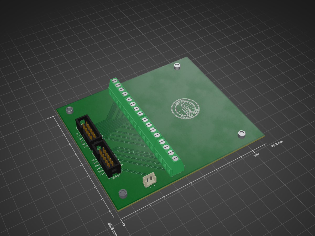
2 layers111.8 × 95.3 mm
 dylanmsu/Splitflap_Display1
software to drive a public split flap display
Splitflap is an open-source printed circuit board by dylanmsu, from the dylanmsu/Splitflap_Display repository on GitHub, published under the GPL-3.0 licence. It is a 2-layer board of 111.8 × 95.3 mm with 12 parts on 18 nets, routed with 56 tracks and 0 vias.
software to digtally drive a public splitflap display using arduino. The display is meant do be deployed in a steamtrain station where it reads the data from their server. This project is still in development and requires major improvements and code cleanup.
The included Arduino compatible library is designed to drive a complete split flap display board with 32 individual modules. There are also methods included to drive the individual split flaps with great control. You can for example call the method:
splitflaps.flipSegment(int segment);That line of code will flip the segment once. Or if you want more control, there is the method:
splitflaps.writeSegment(int segment, int state);It sets the state of the selected h-Bridge. There are (in the future) a bunch of example sketches with different use cases for the library. However, they all require at least one driver PCB to actually drive the split flap modules.
The driver PCBs can drive 8 splitflap modules at the same time, for that it uses 4 SN754410NE chips (L293D in version 4) that are driven by two 74HC595 shift registers. One shift registers drives the H-bridges, the other enables the outputs of the 8 H-Bridges so they dont waste unnecessary power. The communication protocol is quite simple. You have two serial data inputs in the input connector, one is to enable the individual H-Bridges (DiE, ClkE, LaE), the other is to drive the individual H-bridges (Di, Clk, La). They can be daisy-chained to drive an infinite number of splitflap modules.
To actually drive splitflap modules with it, open the arduino sketch named TestDriver. Connect the splitflap modules solenoid connections to the H-Bridge output pairs. Then connect the serial pins to the arduino pins listed in the sketch. and lastly connect 20v to the Vdd input connector. Upload the sketch, the splitflaps should be working.
| Qty | Value | Footprint | References |
|---|---|---|---|
| 4 | Screw_Terminal_01x04 | TerminalBlock:TerminalBlock_bornier-4_P5.08mm | J3, J4, J5, J6 |
| 2 | Conn_02x06_Odd_Even | Connector_IDC:IDC-Header_2x06_P2.54mm_Vertical | J1, J2 |
| 1 | Conn_01x02_Male | Connector_JST:JST_EH_B2B-EH-A_1x02_P2.50mm_Vertical | J7 |
| 1 | LOGO | maldegem:logo_maldegem3 | G*** |
The 8 most common of 12 parts.
It measures 111.8 × 95.3 mm and has 2 copper layers, 1.6 mm thick.
12 parts. The full list of its parts is on this page, with links to each part's symbol and footprint where PCBKit's library has them.
From the dylanmsu/Splitflap_Display repository on GitHub, at the commit this page was made from: the board is hardware/sensor_PCB/splitflap.kicad_pcb. PCBKit opens the board in the browser, with nothing to install.
Its repository publishes it under the GPL-3.0 licence: you may reuse it on that licence's terms (keep the author's notice, and for a copyleft licence share your changes alike).


github-linguist/linguist
Language Savant. If your repository's language is being reported incorrectly, send us a pull request!


google/mozc-devices
Circuit diagrams and firmware source code for Gboard DIY keyboards


hackclub/OnBoard
💡 Join 1,000 teenagers and make your first PCB with a $100 grant!

VoronDesign/Voron-Tap
Tap is a nozzle-based z-probe for the V2 and Trident printer designs. The entire toolhead moves to trigger an optical switch. Tap offers many advantages:

stacksmashing/pico-tpmsniffer
A simple, very experimental TPM sniffer for LPC bus