2 layers242.5 × 87.9 mm
 dycli/petrock
Custom Keyboard
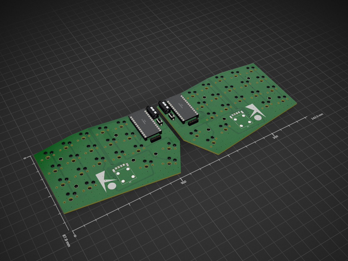
Petrock-40 is an open-source printed circuit board by dycli, from the dycli/petrock repository on GitHub. It is a 2-layer board of 242.5 × 87.9 mm with 102 parts on 94 nets, routed with 542 tracks and 261 vias.
Its parts include 40 diodes, 40 switches, 4 connectors and 2 ICs. It belongs with the keyboards and input boards and the AVR (ATmega, ATtiny) boards of this library.
A split choc keyboard with a trackpoint in place of an outer thumb key: Petrock-41 has one, at the right thumb; Petrock-40 has one on each half; Petrock-42 has none, a key at both outer thumbs.
Based on holykeebs' Corne Choc PCB and plate from
idank/keyboards (corne/choc, commit
f149b9b), licensed CC-BY-SA-4.0. This derivative uses the same licence.
The board is built from the stock file: its parts move to the new layout, and every wire is then drawn afresh by rule (see Build). The stock schematic's connections stay, apart from the thumbs' columns (see Firmware).
tools/no_leds.py). An RGB version may follow.tools/stagger.py;
stock is off by up to 0.02 mm).tools/thumbs.py). The 1.5u inner key becomes two 1u keys;
the new upper one takes the thumb row's last free column (col 0).tools/outer_thumb.py, footprints from tools/make_footprints.py).tools/pins.py).tools/outline.py): a flat top 1.15 mm
above the middle column, 7.5-degree slopes to either side, a straight outer
side, one 7.5-degree bottom edge, and the inner side widened for the upper
thumb key (tools/widen.py). Keycaps sit 1.15 mm from the edge wherever it
follows them.tools/inner_strip.py).tools/stamp.py; the build won't stamp uncommitted
scripts); the board and the switch plates
carry the Petrock logo with a 7 mm dot in its notch (tools/logo.py), and the
jack, reset button and OLED header have no printed outlines
(tools/quiet_silk.py).tools/standoffs.py):
four where four keys meet, each at the four keys' centre, forming a 54 x 34 mm
rectangle (pinky and ring columns, and index and inner index columns, each
between their top two rows and below their third); and one at the thumbs,
equally far from its three keycap corners. A key diode may move a fraction to
make room, if it stays clear. The switch plate has a screw hole over each
(tools/plate.py), as stock.tools/plate.py): the right one (both, on Petrock-40;
neither, on Petrock-42) has an opening for the trackpoint sensor; a new FR4 bottom plate fits the
outline.tools/build.sh [single|dual|none] regenerates a board from the stock file:
tools/parts.py drag).tools/route.py), as a careful hand would: each column a
straight line up the front through its switch pins; each row a line along
the back under its keys, stepping 45 degrees in the gap between columns;
every diode in the same place beside its key with the same two short links;
the column wires gathered into an evenly spaced bus in the gap under the
middle row and fanned into the controller in a staircase; the trackpoint
wires and power in a bundle up the lane between the middle and index
columns and along the top edge; every bend 45 degrees, no right angles
except where a wire joins another. Then ground is poured on both sides and
stitched together with vias (tools/stitch.py).Then tools/plates.sh makes the plates (order the switch plates at 1.2 mm,
which choc switches clip into; the main board and bottom plate at 1.6 mm; all
in HASL, the cheapest finish: the trackpoint driver's pads are hand-soldered
and wide enough that ENIG's flatness isn't needed)
and the 1:1 printout (print it with
scaling off, e.g. lp -o print-scaling=none). tools/fab.sh [single|dual|none]
writes Gerber and drill zips and JLC's assembly BOM and placement (diodes and
hot-swap sockets) to fab/; tools/demo.sh renders demo/. All need KiCad 10.
Outputs: pcb/petrock-41*.kicad_pcb and pcb/bottom.kicad_pcb;
pcb/dual/petrock-40*.kicad_pcb and pcb/dual/bottom.kicad_pcb;
pcb/none/petrock-42*.kicad_pcb and pcb/none/bottom.kicad_pcb.
The stack, per standoff: a top screw through the switch plate's 2.1 mm hole into a spacer that passes through the main board's 3.1 mm hole down to the bottom plate, where a bottom screw holds it. The switch plate and bottom plate clamp the spacers; the main board hangs from the switches (clipped into the plate, pins in the hot-swap sockets), 1.0 mm under the plate.
_r nets): rows 0-2 are the three full rows,
columns 1-5 pinky to inner index. Row 3 is the bottom pinky key (col 1), the
bottom ring key (col 2) and the thumbs, outer to inner: col 3, col 4, col 5.
Col 0 is unused, except on a half with four thumbs (the 41's left, both of
the 42's): there the extra outermost one (in the trackpoint's place) is col
3, the next two col 4 and col 5, and the innermost col 0.SOFT_SERIAL_PIN GP8,
PIO driver); PS/2 PS2_CLOCK_PIN GP0, PS2_DATA_PIN GP1 (PIO driver).| Qty | Value | Footprint | References |
|---|---|---|---|
| 40 | D | kbd:D3_SMD_v2 | D1, D2, D10, D11, D12, D13, D14, D15, D16, D17, D18, D20, D21, D22, D23, D24 +24 |
| 40 | SW_PUSH | holykeebs:SW_choc_v1_HS_CPG135001S30_1u | SW1, SW2, SW10, SW11, SW12, SW13, SW14, SW15, SW16, SW17, SW18, SW20, SW21, SW22, SW23, SW24 +24 |
| 8 | h2 | holykeebs:M2_SPACER | h2, h2, h2, h2, h2, h2, h2, h2 |
| 2 | M2_SPACER | holykeebs:M2_SPACER | , |
| 2 | MJ-4PP-9 | kbd:MJ-4PP-9_1side | J1, J3 |
| 2 | OLED | holykeebs:OLED_1side_1mm_holes | J2, J4 |
| 2 | ProMicro | holykeebs:ProMicro_1mm_holes | U1, U2 |
| 2 | SK8707-01 driver | SK8707-01_driver | A2, A4 |
| 2 | SK8707-01 sensor | SK8707-01_sensor | A1, A3 |
| 2 | SW_PUSH | kbd:ResetSW_1side | RSW1, RSW2 |

pierrechevalier83/ferris
A low profile split keyboard designed to satisfy one single use case elegantly


hackclub/OnBoard
💡 Join 1,000 teenagers and make your first PCB with a $100 grant!


newdigate/teensy-eurorack
Hardware Design: Eurorack shield for teensy 4.1 with 14 in / 16 out analog channels


It measures 242.5 × 87.9 mm and has 2 copper layers, 1.6 mm thick.
102 parts. The full list of its parts is on this page, with links to each part's symbol and footprint where PCBKit's library has them.
From the dycli/petrock repository on GitHub, at the commit this page was made from: the board is pcb/dual/petrock-40.kicad_pcb and its schematic pcb/petrock-41.kicad_sch. PCBKit opens the board in the browser, with nothing to install.
Its repository states no licence, so its author keeps all rights: ask dycli before reusing the design.